【转】PCIE 通道x4/8/16的定义
|
PCI Express 版本 |
行代码 |
传输速率 |
吞吐量 |
|||
|
×1 |
×4 |
×8 |
×16 |
|||
|
1.0 |
8b/10b |
2.5GT/s |
250MB/s |
1GB/s |
2GB/s |
4GB/s |
|
2.0 |
8b/10b |
5GT/s |
500MB/s |
2GB/s |
4GB/s |
8GB/s |
|
3.0 |
128b/130b |
8GT/s |
984.6MB/s |
3.938GB/s |
7.877GB/s |
15.754GB/s |
|
4.0 |
128b/130b |
16GT/s |
1.969GB/s |
7.877GB/s |
15.754GB/s |
31.508GB/s |
|
5.0 |
128b/130b |
32 or 25GT/s |
3.9 or 3.08GB/s |
15.8 or 12.3GB/s |
31.5 or 24.6GB/s |
63.0 or 49.2GB/s |
PCI-Express(peripheral component interconnect express)是一种高速串行计算机扩展总线标准,它原来的名称为“3GIO”,是由英特尔在2001年提出的,旨在替代旧的PCI,PCI-X和AGP总线标准。PCIe属于高速串行点对点双通道高带宽传输
PCI-E gen3的定义
1)PCI-E3.0,速度是8Gbps,GEN3是第三代;
2)一个通道即一个lane就是一对rx和tx,PCI-E ×4 就是4个lane或者加个switch。
https://pinouts.ru/Slots/pci_express_pinout.shtml
PCI Express (PCIe, PCI-e) is a high-speed serial computer expansion bus standard.
PCI Express as a high-bandwidth, low pin count, serial, interconnect technology. It was designed to replace the older PCI and AGPbus standards. PCIe has numerous improvements over the older standards, including higher maximum system bus throughput, lower I/O pin count and smaller physical footprint, better performance scaling for bus devices, a more detailed error detection and reporting mechanism (Advanced Error Reporting, AER), and native hot-swap functionality. PCI Express architecture provides a high performance I/O infrastructure for Desktop Platforms with transfer rates starting at 2.5 Giga transfers per second over a x1 PCI Express lane for Gigabit Ethernet, TV Tuners, Firewire 1394a/b controllers, and general purpose I/O. PCI Express architecture provides a high performance graphics infrastructure for Desktop Platforms doubling the capability of existing AGP8x designs with transfer rates of 4.0 Gigabytes per second over a x16 PCI Express lane for graphics controllers. A lane is composed of two differential signaling pairs, with one pair for receiving data and the other for transmitting.
ExpressCard utilizing PCI Express interface, developed by the PCMCIA group for mobile computers. PCI Express Advanced Power Management features help to extend platform battery life and to enable users to work anywhere, without an AC power source. The PCI Express electrical interface is also used in some computer storage interfaces SATA Express and M.2.
The broad adoption of PCI Express in the mobile, enterprise and communication segments enables convergence through the re-use of a common interconnect technology.
PCI-E is a serial bus which uses two low-voltage differential LVDS pairs, at 2.5Gb/s in each direction [one transmit, and one receive pair]. PCI Express supports 1x [2.5Gbps], 2x, 4x, 8x, 12x, 16x, and 32x bus widths [transmit / receive pairs].
The differential pins [Lanes] listed in the pin out table above are LVDS which stands for: Low Voltage Differential Signaling.
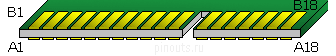
PCI-Express 1x Connector Pin-Out
| Pin |
Side B Connector |
Side A Connector |
||
| # | Name | Description | Name | Description |
| 1 | +12v | +12 volt power | PRSNT#1 | Hot plug presence detect |
| 2 | +12v | +12 volt power | +12v | +12 volt power |
| 3 | +12v | +12 volt power | +12v | +12 volt power |
| 4 | GND | Ground | GND | Ground |
| 5 | SMCLK | SMBus clock | JTAG2 | TCK |
| 6 | SMDAT | SMBus data | JTAG3 | TDI |
| 7 | GND | Ground | JTAG4 | TDO |
| 8 | +3.3v | +3.3 volt power | JTAG5 | TMS |
| 9 | JTAG1 | +TRST# | +3.3v | +3.3 volt power |
| 10 | 3.3Vaux | 3.3v volt power | +3.3v | +3.3 volt power |
| 11 | WAKE# | Link Reactivation | PWRGD | Power Good |
|
Mechanical Key |
||||
| 12 | RSVD | Reserved | GND | Ground |
| 13 | GND | Ground | REFCLK+ |
Reference Clock Differential pair |
| 14 | HSOp(0) |
Transmitter Lane 0, Differential pair |
REFCLK- | |
| 15 | HSOn(0) | GND | Ground | |
| 16 | GND | Ground | HSIp(0) |
Receiver Lane 0, Differential pair |
| 17 | PRSNT#2 | Hotplug detect | HSIn(0) | |
| 18 | GND | Ground | GND | Ground |
====================================================================
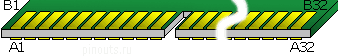
PCI-Express 4x Connector Pin-Out
| Pin |
Side B Connector |
Side A Connector |
||
| # | Name | Description | Name | Description |
| 1 | +12v | +12 volt power | PRSNT#1 | Hot plug presence detect |
| 2 | +12v | +12 volt power | +12v | +12 volt power |
| 3 | +12v | +12 volt power | +12v | +12 volt power |
| 4 | GND | Ground | GND | Ground |
| 5 | SMCLK | SMBus clock | JTAG2 | TCK |
| 6 | SMDAT | SMBus data | JTAG3 | TDI |
| 7 | GND | Ground | JTAG4 | TDO |
| 8 | +3.3v | +3.3 volt power | JTAG5 | TMS |
| 9 | JTAG1 | +TRST# | +3.3v | +3.3 volt power |
| 10 | 3.3Vaux | 3.3v volt power | +3.3v | +3.3 volt power |
| 11 | WAKE# | Link Reactivation | PWRGD | Power Good |
|
Mechanical Key |
||||
| 12 | RSVD | Reserved | GND | Ground |
| 13 | GND | Ground | REFCLK+ |
Reference Clock Differential pair |
| 14 | HSOp(0) |
Transmitter Lane 0, Differential pair |
REFCLK- | |
| 15 | HSOn(0) | GND | Ground | |
| 16 | GND | Ground | HSIp(0) |
Receiver Lane 0, Differential pair |
| 17 | PRSNT#2 | Hotplug detect | HSIn(0) | |
| 18 | GND | Ground | GND | Ground |
| 19 | HSOp(1) |
Transmitter Lane 1, Differential pair |
RSVD | Reserved |
| 20 | HSOn(1) | GND | Ground | |
| 21 | GND | Ground | HSIp(1) |
Receiver Lane 1, Differential pair |
| 22 | GND | Ground | HSIn(1) | |
| 23 | HSOp(2) |
Transmitter Lane 2, Differential pair |
GND | Ground |
| 24 | HSOn(2) | GND | Ground | |
| 25 | GND | Ground | HSIp(2) |
Receiver Lane 2, Differential pair |
| 26 | GND | Ground | HSIn(2) | |
| 27 | HSOp(3) |
Transmitter Lane 3, Differential pair |
GND | Ground |
| 28 | HSOn(3) | GND | Ground | |
| 29 | GND | Ground | HSIp(3) |
Receiver Lane 3, Differential pair |
| 30 | RSVD | Reserved | HSIn(3) | |
| 31 | PRSNT#2 | Hot plug detect | GND | Ground |
| 32 | GND | Ground | RSVD | Reserved |
====================================================================
PCI-Express 8x Connector Pin-Out

| Pin |
Side B Connector |
Side A Connector |
||
| # | Name | Description | Name | Description |
| 1 | +12v | +12 volt power | PRSNT#1 | Hot plug presence detect |
| 2 | +12v | +12 volt power | +12v | +12 volt power |
| 3 | +12v | +12 volt power | +12v | +12 volt power |
| 4 | GND | Ground | GND | Ground |
| 5 | SMCLK | SMBus clock | JTAG2 | TCK |
| 6 | SMDAT | SMBus data | JTAG3 | TDI |
| 7 | GND | Ground | JTAG4 | TDO |
| 8 | +3.3v | +3.3 volt power | JTAG5 | TMS |
| 9 | JTAG1 | +TRST# | +3.3v | +3.3 volt power |
| 10 | 3.3Vaux | 3.3v volt power | +3.3v | +3.3 volt power |
| 11 | WAKE# | Link Reactivation | PWRGD | Power Good |
|
Mechanical Keycard |
||||
| 12 | RSVD | Reserved | GND | Ground |
| 13 | GND | Ground | REFCLK+ |
Reference Clock Differential pair |
| 14 | HSOp(0) |
Transmitter Lane 0, Differential pair |
REFCLK- | |
| 15 | HSOn(0) | GND | Ground | |
| 16 | GND | Ground | HSIp(0) |
Receiver Lane 0, Differential pair |
| 17 | PRSNT#2 | Hotplug detect | HSIn(0) | |
| 18 | GND | Ground | GND | Ground |
| 19 | HSOp(1) |
Transmitter Lane 1, Differential pair |
RSVD | Reserved |
| 20 | HSOn(1) | GND | Ground | |
| 21 | GND | Ground | HSIp(1) |
Receiver Lane 1, Differential pair |
| 22 | GND | Ground | HSIn(1) | |
| 23 | HSOp(2) |
Transmitter Lane 2, Differential pair |
GND | Ground |
| 24 | HSOn(2) | GND | Ground | |
| 25 | GND | Ground | HSIp(2) |
Receiver Lane 2, Differential pair |
| 26 | GND | Ground | HSIn(2) | |
| 27 | HSOp(3) |
Transmitter Lane 3, Differential pair |
GND | Ground |
| 28 | HSOn(3) | GND | Ground | |
| 29 | GND | Ground | HSIp(3) |
Receiver Lane 3, Differential pair |
| 30 | RSVD | Reserved | HSIn(3) | |
| 31 | PRSNT#2 | Hot plug detect | GND | Ground |
| 32 | GND | Ground | RSVD | Reserved |
| 33 | HSOp(4) |
Transmitter Lane 4, Differential pair |
RSVD | Reserved |
| 34 | HSOn(4) | GND | Ground | |
| 35 | GND | Ground | HSIp(4) |
Receiver Lane 4, Differential pair |
| 36 | GND | Ground | HSIn(4) | |
| 37 | HSOp(5) |
Transmitter Lane 5, Differential pair |
GND | Ground |
| 38 | HSOn(5) | GND | Ground | |
| 39 | GND | Ground | HSIp(5) |
Receiver Lane 5, Differential pair |
| 40 | GND | Ground | HSIn(5) | |
| 41 | HSOp(6) |
Transmitter Lane 6, Differential pair |
GND | Ground |
| 42 | HSOn(6) | GND | Ground | |
| 43 | GND | Ground | HSIp(6) |
Receiver Lane 6, Differential pair |
| 44 | GND | Ground | HSIn(6) | |
| 45 | HSOp(7) |
Transmitter Lane 7, Differential pair |
GND | Ground |
| 46 | HSOn(7) | GND | Ground | |
| 47 | GND | Ground | HSIp(7) |
Receiver Lane 7, Differential pair |
| 48 | PRSNT#2 | Hot plug detect | HSIn(7) | |
| 49 | GND | Ground | GND | Ground |
====================================================================
PCI-Express 16x Connector Pin-Out

| Pin |
Side B Connector |
Side A Connector |
||
| # | Name | Description | Name | Description |
| 1 | +12v | +12 volt power | PRSNT#1 | Hot plug presence detect |
| 2 | +12v | +12 volt power | +12v | +12 volt power |
| 3 | +12v | +12 volt power | +12v | +12 volt power |
| 4 | GND | Ground | GND | Ground |
| 5 | SMCLK | SMBus clock | JTAG2 | TCK |
| 6 | SMDAT | SMBus data | JTAG3 | TDI |
| 7 | GND | Ground | JTAG4 | TDO |
| 8 | +3.3v | +3.3 volt power | JTAG5 | TMS |
| 9 | JTAG1 | +TRST# | +3.3v | +3.3 volt power |
| 10 | 3.3Vaux | 3.3v volt power | +3.3v | +3.3 volt power |
| 11 | WAKE# | Link Reactivation | PWRGD | Power Good |
|
Mechanical Key |
||||
| 12 | RSVD | Reserved | GND | Ground |
| 13 | GND | Ground | REFCLK+ |
Reference Clock Differential pair |
| 14 | HSOp(0) |
Transmitter Lane 0, Differential pair |
REFCLK- | |
| 15 | HSOn(0) | GND | Ground | |
| 16 | GND | Ground | HSIp(0) |
Receiver Lane 0, Differential pair |
| 17 | PRSNT#2 | Hotplug detect | HSIn(0) | |
| 18 | GND | Ground | GND | Ground |
| 19 | HSOp(1) |
Transmitter Lane 1, Differential pair |
RSVD | Reserved |
| 20 | HSOn(1) | GND | Ground | |
| 21 | GND | Ground | HSIp(1) |
Receiver Lane 1, Differential pair |
| 22 | GND | Ground | HSIn(1) | |
| 23 | HSOp(2) |
Transmitter Lane 2, Differential pair |
GND | Ground |
| 24 | HSOn(2) | GND | Ground | |
| 25 | GND | Ground | HSIp(2) |
Receiver Lane 2, Differential pair |
| 26 | GND | Ground | HSIn(2) | |
| 27 | HSOp(3) |
Transmitter Lane 3, Differential pair |
GND | Ground |
| 28 | HSOn(3) | GND | Ground | |
| 29 | GND | Ground | HSIp(3) |
Receiver Lane 3, Differential pair |
| 30 | RSVD | Reserved | HSIn(3) | |
| 31 | PRSNT#2 | Hot plug detect | GND | Ground |
| 32 | GND | Ground | RSVD | Reserved |
| 33 | HSOp(4) |
Transmitter Lane 4, Differential pair |
RSVD | Reserved |
| 34 | HSOn(4) | GND | Ground | |
| 35 | GND | Ground | HSIp(4) |
Receiver Lane 4, Differential pair |
| 36 | GND | Ground | HSIn(4) | |
| 37 | HSOp(5) |
Transmitter Lane 5, Differential pair |
GND | Ground |
| 38 | HSOn(5) | GND | Ground | |
| 39 | GND | Ground | HSIp(5) |
Receiver Lane 5, Differential pair |
| 40 | GND | Ground | HSIn(5) | |
| 41 | HSOp(6) |
Transmitter Lane 6, Differential pair |
GND | Ground |
| 42 | HSOn(6) | GND | Ground | |
| 43 | GND | Ground | HSIp(6) |
Receiver Lane 6, Differential pair |
| 44 | GND | Ground | HSIn(6) | |
| 45 | HSOp(7) |
Transmitter Lane 7, Differential pair |
GND | Ground |
| 46 | HSOn(7) | GND | Ground | |
| 47 | GND | Ground | HSIp(7) |
Receiver Lane 7, Differential pair |
| 48 | PRSNT#2 | Hot plug detect | HSIn(7) | |
| 49 | GND | Ground | GND | Ground |
| 50 | HSOp(8) |
Transmitter Lane 8, Differential pair |
RSVD | Reserved |
| 51 | HSOn(8) | GND | Ground | |
| 52 | GND | Ground | HSIp(8) |
Receiver Lane 8, Differential pair |
| 53 | GND | Ground | HSIn(8) | |
| 54 | HSOp(9) |
Transmitter Lane 9, Differential pair |
GND | Ground |
| 55 | HSOn(9) | GND | Ground | |
| 56 | GND | Ground | HSIp(9) |
Receiver Lane 9, Differential pair |
| 57 | GND | Ground | HSIn(9) | |
| 58 | HSOp(10) |
Transmitter Lane 10, Differential pair |
GND | Ground |
| 59 | HSOn(10) | GND | Ground | |
| 60 | GND | Ground | HSIp(10) |
Receiver Lane 10, Differential pair |
| 61 | GND | Ground | HSIn(10) | |
| 62 | HSOp(11) |
Transmitter Lane 11, Differential pair |
GND | Ground |
| 63 | HSOn(11) | GND | Ground | |
| 64 | GND | Ground | HSIp(11) |
Receiver Lane 11, Differential pair |
| 65 | GND | Ground | HSIn(11) | |
| 66 | HSOp(12) |
Transmitter Lane 12, Differential pair |
GND | Ground |
| 67 | HSOn(12) | GND | Ground | |
| 68 | GND | Ground | HSIp(12) |
Receiver Lane 12, Differential pair |
| 69 | GND | Ground | HSIn(12) | |
| 70 | HSOp(13) |
Transmitter Lane 13, Differential pair |
GND | Ground |
| 71 | HSOn(13) | GND | Ground | |
| 72 | GND | Ground | HSIp(13) |
Receiver Lane 13, Differential pair |
| 73 | GND | Ground | HSIn(13) | |
| 74 | HSOp(14) |
Transmitter Lane 14, Differential pair |
GND | Ground |
| 75 | HSOn(14) | GND | Ground | |
| 76 | GND | Ground | HSIp(14) |
Receiver Lane 14, Differential pair |
| 77 | GND | Ground | HSIn(14) | |
| 78 | HSOp(15) |
Transmitter Lane 15, Differential pair |
GND | Ground |
| 79 | HSOn(15) | GND | Ground | |
| 80 | GND | Ground | HSIp(15) |
Receiver Lane 15, Differential pair |
| 81 | PRSNT#2 | Hot plug present detect | HSIn(15) | |
| 82 | RSVD#2 | Hot Plug Detect | GND | Ground |
PRSNT#1 is connected to GND on motherboard.
Add on card needs to have PRSNT#1 connected to one of PRSNT#2 depending what type of connector is in use.
PCI-express standards
PCI Express 1.0a
In 2003, PCI-SIG introduced PCIe 1.0a, with a per-lane data rate of 250 MB/s and a transfer rate of 2.5 gigatransfers per second (GT/s). Transfer rate is expressed in transfers per second instead of bits per second because the number of transfers includes the overhead bits, which do not provide additional throughput; PCIe 1.x uses an 8b/10b encoding scheme, resulting in a 20% (= 2/10) overhead on the raw channel bandwidth.
PCI Express 2.0
PCI-SIG announced the availability of the PCI Express Base 2.0 specification on 15 January 2007. The PCIe 2.0 standard doubles the transfer rate compared with PCIe 1.0 to 5 GT/s and the per-lane throughput rises from 250 MB/s to 500 MB/s. Consequently, a 32-lane PCIe connector (×32) can support an aggregate throughput of up to 16 GB/s. PCIe 2.0 motherboard slots are fully backward compatible with PCIe v1.x cards. PCIe 2.0 cards are also generally backward compatible with PCIe 1.x motherboards, using the available bandwidth of PCI Express 1.1. Overall, graphic cards or motherboards designed for v2.0 will work with the other being v1.1 or v1.0a. Like 1.x, PCIe 2.0 uses an 8b/10b encoding scheme, therefore delivering, per-lane, an effective 4 Gbit/s max transfer rate from its 5 GT/s raw data rate.
PCI Express 2.1
PCI Express 2.1 (dated March 4, 2009) supports a large proportion of the management, support, and troubleshooting systems planned for full implementation in PCI Express 3.0. However, the speed is the same as PCI Express 2.0. The increase in power from the slot breaks backward compatibility between PCI Express 2.1 cards and some older motherboards with 1.0/1.0a, but most motherboards with PCI Express 1.1 connectors are provided with a BIOS update by their manufacturers through utilities to support backward compatibility of cards with PCIe 2.1.
PCI Express 3.0
PCI Express 3.0 specification was made available in November 2010. New features for the PCI Express 3.0 specification include a number of optimizations for enhanced signaling and data integrity, including transmitter and receiver equalization, PLL improvements, clock data recovery, and channel enhancements for currently supported topologies. PCI Express 3.0 upgrades the encoding scheme to 128b/130b from the previous 8b/10b encoding, reducing the bandwidth overhead from 20% of PCI Express 2.0 to approximately 1.54% (= 2/130). This is achieved by XORing a known binary polynomial as a scrambler to the data stream in a feedback topology. PCI Express 3.0's 8 GT/s bit rate effectively delivers 985 MB/s per lane, nearly doubling the lane bandwidth relative to PCI Express 2.0.
PCI Express 4.0
PCI Express 4.0 was officially announced on 2017, providing a 16 GT/s bit rate that doubles the bandwidth provided by PCI Express 3.0, while maintaining backward and forward compatibility in both software support and used mechanical interface. PCI Express 4.0 specs will also bring OCuLink-2, an alternative to Thunderbolt connector. OCuLink version 2 will have up to 16 GT/s (8 GB/s total for ×4 lanes), while the maximum bandwidth of a Thunderbolt 3 connector is 5 GB/s. Additionally, active and idle power optimizations are to be investigated.
【转】PCIE 通道x4/8/16的定义相关推荐
- 缠绕多年的PCIE通道数问题终于完全明白了,欢迎指正
CPU的PCIE通道数,之前一直都是一个众说纷纭的问题 很多人都会问到,主板上不同的M.2接口,接SSD性能是否一样,接太多的SSD,是否会占用显卡的PCIE带宽,今天我又看了几篇网上的文章,终于十分 ...
- 常见PCIE X1/X4/X8/X16插槽作用与区别
一.现在PCI-E插槽已经成为了主板上的主力扩展插槽.基本集中在PCI-E x1/x4/x8/x16四种上,有何作用? 具体作用是: 1.显卡会用到PCI-E插槽.PCI-E 3.0 x16能够满足任 ...
- pcie总线连接两台电脑_【PCI-E通道是个什么东西?他是干啥的?】
前言: 经常接触台式机的同学肯定绕不开PCI-E这个名词,因为这是台式机里最重要的接口/通道之一,就算是笔记本,也有很多地方会提到,就好比你加固态硬盘的时候,查阅资料的时候你应该会发现有的M.2接口走 ...
- PCI-E x1/x4/x8/x16四种插槽区别是什么
我们知道,为了满足工业使用领域的扩展需要,工控机都会配备PCIe插槽,PCIe属于高速串行点对点双通道高带宽传输,所连接的设备分配独享通道带宽,不共享总线带宽,主要支持主动电源管理,错误报告,端对端的 ...
- FMC子卡:4 通道 250MSPS采样率16 位 AD 采集子卡
FMC136 是一款 4 通道 250MHz 采样率 16 位 AD 采集 FMC子卡,符合 VITA57 规范,可以作为一个理想的 IO 模块耦合至FPGA前端,4 通道 AD 通过高带宽的 FMC ...
- FMC子卡:8 通道 125MSPS采样率16 位 AD 采集子卡
FMC129 是一款 8 通道 125MHz 采样率 16 位 AD 采集 FMC 子卡,符合 VITA57.1 规范,可以作为一个理想的 IO 模块耦合至 FPGA前端,8 通道 AD 通过高带宽的 ...
- 8通道250MSPS采样率16位AD采集FMC子卡-高速数据采集专家
FMC128是一款8通道250MHz采样率16位分辨率AD采集FMC子卡,符合VITA57.1规范,可以作为一个理想的IO模块耦合至FPGA前端,8通道AD将模拟信号数字化后通过高带宽的FMC连接器( ...
- linux多个pcie设备同时访问,linux – 是否可以写入在同一PCIe插槽上使用不同PCIe通道的多个设备?...
我正在编写一个支持多个设备的Linux设备驱动程序.我有一个x8 PCIe卡,上面有4个这样的设备.每个都通过PCIe交换机运行并获得2个PCIe通道.有没有办法让驱动程序同时写入多个通道?如果是这样 ...
- 【转载】PCI-E接口以及PCI-E 1x, 4x, 8x, 16x 接口定义
1. PCI-E插槽及金手指实物图 (1)PCI-E插槽 从上至下依次为PCI-E 4X.PCI-E 16X.PCI-E 1X (2)PCI-E金手指 PCI-E 1X金手指 PCI-E 4X金手指 ...
最新文章
- 形态学图像处理或能帮助实例分割
- c++ 迭代器支持的运算
- 微型计算机kong控制技术,AT89C2051单片机在步进电机控制中的应用
- java8获取当前时间并格式化
- Windows phone 8 学习笔记(7) 设备
- UK Biobank专题
- 2019 CCPC 秦皇岛F Forest Program(dfs)
- linux blind函数,C++拾遗--bind函数绑定
- 移动设备尚未形成DDoS的3个原因
- 陈绪:3月21日阿里云北京峰会专场出品人
- 基于大数据的京沪人口流动流量、流向新变化
- linux 批量修改文件后缀名
- 人工智能——特征工程思维导图
- 【Deepin】 Deepin 系统安装教程
- 最新易支付多功能系统源码+全开源
- 音频在计算机里存储形式是什么,如何在录音带上存储任何类型的文件
- linux鼠标切换窗口的快捷键设置,Xshell中如何设置鼠标快捷键
- 使用小波包变换分析信号的matlab程序,使用小波包变换分析信号的MATLAB程序
- Java13新增特性
- 如何在matlab中表达点集,matlab练习程序(点集配准的SVD法)