FPGA基础知识21(PL控制PS端DDR的设计)
来自:http://www.eefocus.com/antaur/blog/17-08/423773_0818c.html
0.引言
构建SoC系统,毕竟是需要实现PS和PL间的数据交互,而像上一讲那样PL主机与PL从机之间通过AXI4-Lite总线进行交互有点杀鸡用牛刀了。
如果PS与PL端进行数据交互,可以直接设计PL端为从机,PS端向PL端的reg写入数据即可,但是对于图像处理等大数据量的数据交互来说,PL端的BRAM毕竟容量有限,很难用BRAM作为两者间的数据缓存器。对于这样的应用来说,利用DDR3作为PS端与PL端之间交互的数据缓存器是最合适不过的。(当然,对于大数据量的数据交互,利用AXI4-Lite总线模式效率太低,最佳选择是AXI4-Stream,这是后话,后面在进行研究。)
学习笔记3已经实现了PS端对DDR3的读写操作,本节研究如何再实现PL端对DDR3的读写操作,当然了在真正的工程系统中,还需要设计良好的读写同步,防止竞争冲突,这就属于系统设计层面的了,我再这里暂时忽略不考虑。
本节暂时不涉及PS端对DDR3的操作,而仅仅研究PL端如何对DDR3进行读写操作。
1.工程规划
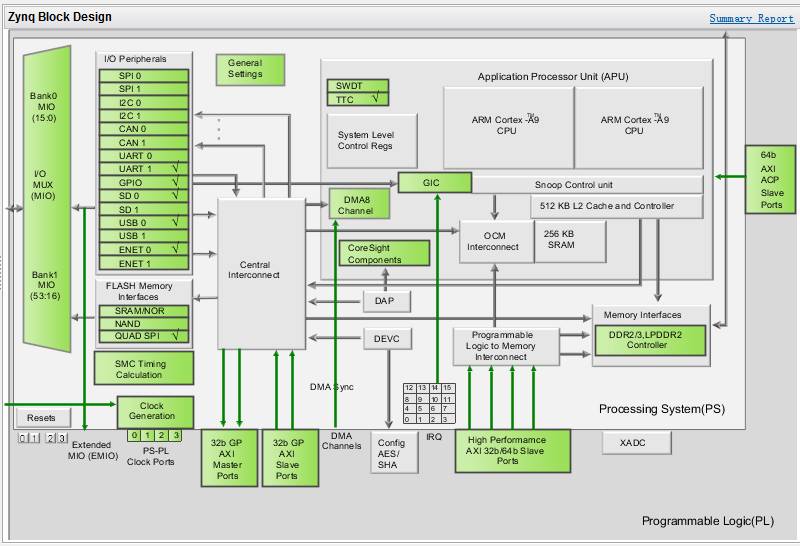
再ZedBoard板子的硬件设计方案中,DDR芯片的管脚是绑定到Zynq的DDR接口上的。
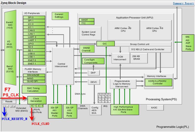
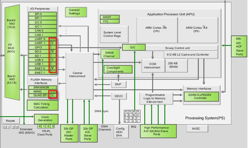
而Zynq系统的这个DDR总线接口有是链接在其内部“Memory Interfaces”中的“DDR2/3,LPDDR2 Controller”可配置硬核上的。
因此,要想PL访问板上的DDR3存储器,必须借道Zynq中的“Memory Interfaces----DDR2/3,LPDDR2 Controller”(后文简称“DDR3 Controller”)。根据之前的经验,在Zynq系统中,ARM Core(CPU)能够访问硬核“DDR3 Controller”,根据经验可以确定“DDR3 Controller”一定是一个从设备,而PL要想访问“DDR3 Controller”的话,PL一定要是一个主设备,由PL发起读写操作。
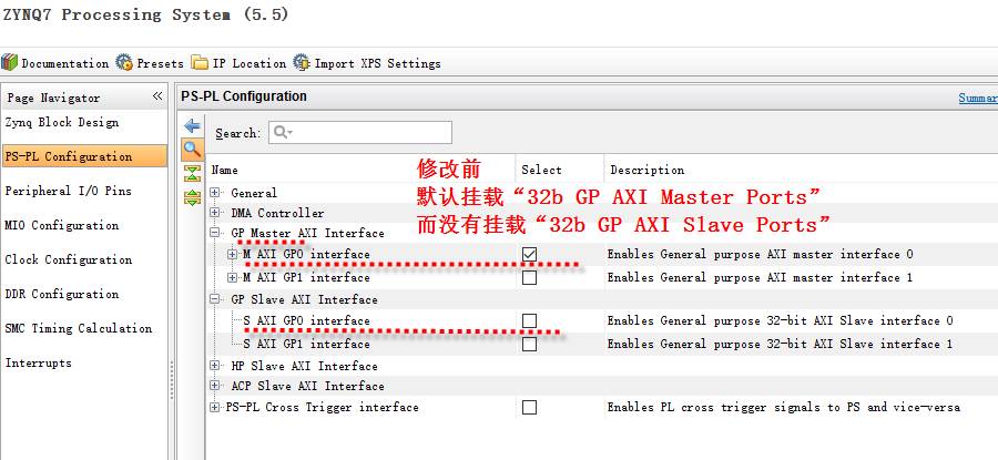
“DDR3 Controller”是封装在Zynq子系统中的,因此,PL必须连接Zynq的从机接口。从上图可以看出,Zynq有两个从机接口,分别是“32b GP AXI Slave Ports”和“High Performance AXI 32b/64b Slave Ports”根据名称可以看出,一个是高性能的,另一个应该是普通的。之前Zynq作为主机连接AXI4-Lite从设备时,走的是“32b GP AXI Master Ports”,可以辅助证明,对于本节应用,走的接口应该是“32b GP AXI Slave Ports”。
交互数据将会经过Zynq子系统的内部总线(用空再考证一下是什么名称)控制器“Central Interconnect”转发给Memory Interfaces。具体数据交互路径如下图所示:
根据上述分析,SoC系统集成方案框图如下:
根据之前的经验,利用向导生成的PL端AXI4-Lite Master IP 用户用例再txn负脉冲触发下,主机模块的逻辑是连续4次(次数默认为4,可通过修改参数C_M00_AXI_TRANSACTIONS_NUM的数值改变次数)向递增的地址区间写入4组测试数据,测试数据每次加1。然后主机模块自动读取刚才写入数据的地址内的数据,将读的的数据与写入数据进行比较,如果正确,主机IP的ERROR信号保持低电平,如果错误,ERROR给出高电平。
本文后面的行为仿真证明:再次给主机IP模块一个txn的触发信号,重新执行4次写入操作+4次读取操作+比较操作。只不过每次触发都从原始基地址开始操作,目标寄存器地址并不增加。
本节的测试工程本着少改动逻辑代码的原则,仍基本采用此逻辑。每次按键触发,执行4次写操作+4次读操作+比对检查操作,增加利用4个LED灯表示每个地址比对结果是否正确(如果正确LED灯亮)。但是当再次按下按钮,LED灯全灭,松开按钮后再执行一组(4次写操作+4次读操作+比对检查)操作,只是新的一组操作地址会递进增加。
2.Zynq系统裁剪
创建工程后,添加一个Zynq IP核,然后调用官方对ZedBoard板中Zynq子系统的默认配置。
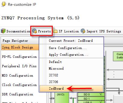
得到默认的Zynq硬核配置如下图所示:
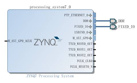
对应的Zynq封装如下图所示:
明显看出有很多Zynq中的硬核在本项目中是不需要的,修改配置,将其裁剪掉。
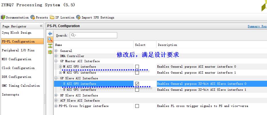
修改后的Zynq配置显示如下:
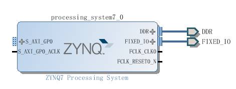
Zynq的封装图如下所示:
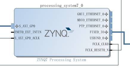
输出端的FCLK_CLK0和FCLK_RESET0_N是输出时钟和复位信号。这两个信号的出处已在前一个图中进行标注。
ZedBoard开发板的ARM端时钟由IC18有源晶振提供33.33333MHz的时钟信号,绑定到Zynq芯片的F7(PS_CLK)管脚上,该管脚是Zynq子系统(PS)的时钟信号。如果工程中添加了Zynq子系统,Vivado会自动将F7绑定到Zynq子系统的PS_CLK管脚上(其实也不需要绑定,这是固话的。F7本身就是专用引脚,但是从硬件结构上也可以看出一个工程只能实例化一个Zynq子系统)。该绑定在约束文件上看不到,而在“Synthesis Design”的“I/O Planning”页面中可以看到。(因为这个管脚是专用管脚,不需要绑定)这里欠个图,后文会有,记着啊!!!
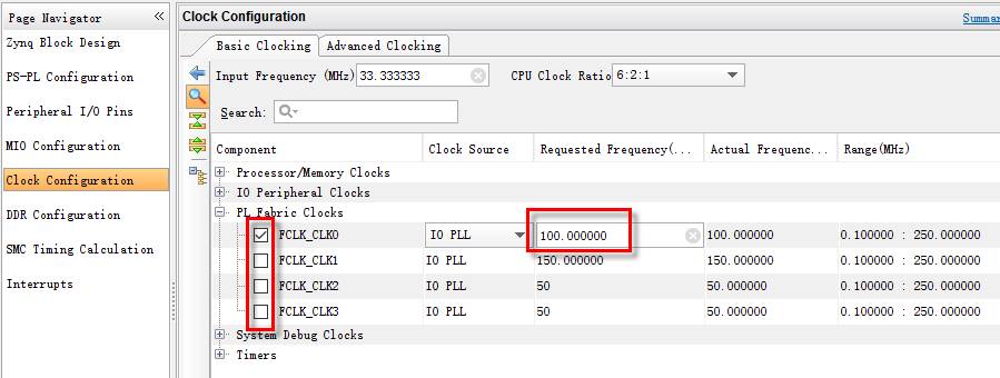
FCLK_CLK0是经过一个时钟管理模块(类似V4中的DCM)生成的,可以修改其参数。Zynq中包含了4个时钟生成模块。配置界面如下:
如果取消勾选,Zynq将不输出时钟信号。
那对于PL端的时序逻辑模块,需要另外寻找时钟信号,在ZedBoard开发板上,IC17有源晶振提供100MHz的GCLK时钟信号,连接到Y9上,可用PL端使用。但是这种方案PS端和PL端由独立的时钟分别驱动,必须考虑跨时钟域问题。
取消FCLK_CLK0的勾选后,Zynq的封装图如下所示:
FCLK_CLK0管脚就没有了,但是FCLK_RESET0_N仍然存在,因为Zynq中的Resets模块是不可配置的。但是Resets有四路输出,为什么这里只有1个呢?是不是跟FCLK_CLKx有绑定呢?
【添加,事后发现,FCLK_RESET0_N也是可以关闭的,操作如下】
太强大的软件了,永远别觉得自己学明白了!!!
为了验证上述疑问,勾选两路FCLK_CLK0和FCLK_CLK2,观察之后的Zynq模块封装如下所示:
没有唤出其余的几路Resets信号。如何召唤其他几路复位信号,还得研究研究。
【个人猜想】:这个FCLK_RESET0_N应该是跟Zynq子系统的复位工作是同步的,有可能Zynq子系统收到复位信号(PS-RST,BTN7,C9,低电平复位)后,FCLK_RESET0_N被拉低,等待一定时间保证Zynq子系统复位完成后,再延时一段时间,再拉高,是的PL端的模块完成复位进入正常工作状态时,Zynq子系统一定已经正常工作。
本项目中,Zynq子系统裁剪完毕后,封装图采用下图方案。
利用FCLK_CLK0驱动PL端的时序逻辑。而将Y9管脚引入的100MHzGCLK信号旁路。
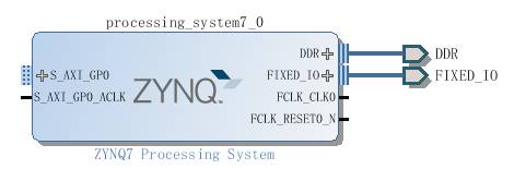
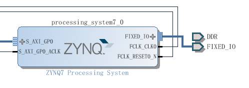
再来看看S_AXI_GP0,即AXI4总线接口(兼容AXI4-Lite)。如下图所示:
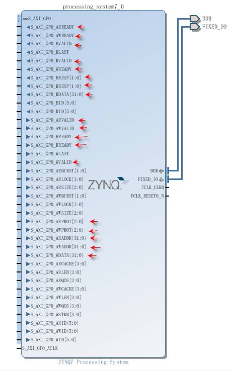
终于,画箭头的管脚我们都熟悉了。其他的以后再说。
至此,Zynq子系统我们裁剪完毕了。
【还有个问题】:“DDR3 Controller”硬核在Zynq子系统内部的内存映射还没有看到。打开Address Editor页面,也没有配置信息。
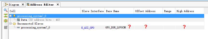
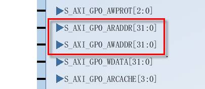
另外,作为从机接口,读写地址总线均为32bits,而不像之前的验证方案,从机的读写地址去掉高位的段地址只留下低位的offset Address,这样的地址接口,能跟PL端的AXI InterConnect匹配吗?
3.PL端主机IP核设计编码
根据之前的经验,利用向导生成一个AXI4-Lite Master IP示例代码,构建主从模块直连的测试系统,从机模块默认内部寄存器数量为4个,构建本仿真系统时,将从机模块内部寄存器数量设置为32个,其余不用修改。
功能仿真文件(详见附录2),模拟连续两次触发txn信号,设置参数,每次txn触发执行两次写读操作,对应的仿真结果如下图所示。
每次txn触发,起始地址均归零,即恢复成初始地址0x4000_0000,写入的数据也变为初始值0xaa00_0000。跟工程设计的逻辑需求不一致。
因此根据需求改造代码逻辑,底层模块的源码详见附录。编码时一定避免Multi-Driver禁告。修改后的逻辑仿真结果如下所示。
可也看出主机模块的功能满足设计要求。
之后将该IP核加入到工程的IP Catalog中。
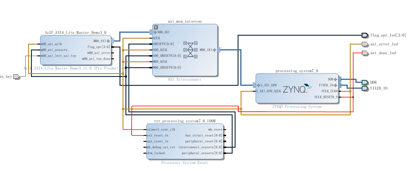
4.在Block Design中增加PL端IP核
首先在Block Design中实例化一个AzIP_AXI_Master_3的一个IP模块,如下图所示,此时没有连接。
点击页面上的Run Connection Audomation按钮,自动创建连接。整形以后如下图所示。新加的两个模块都是老朋友了,基本逻辑核管脚时序都基本明确了。此时再来看这个连接,基本上就没有问题了。图中用彩色标注出了PL端的时钟信号和复位信号。均由Zynq子系统产生。
同样按F6键检查连接,如果检查无误,表示这个系统的“原理图”画的基本没有问题了。
5.内存映射分析
点击Address Editor标签,看一看,这个图前文在zynq子系统配置完后曾经出现过,但是当时是没有数据的,现在我们放在一起对比一下:
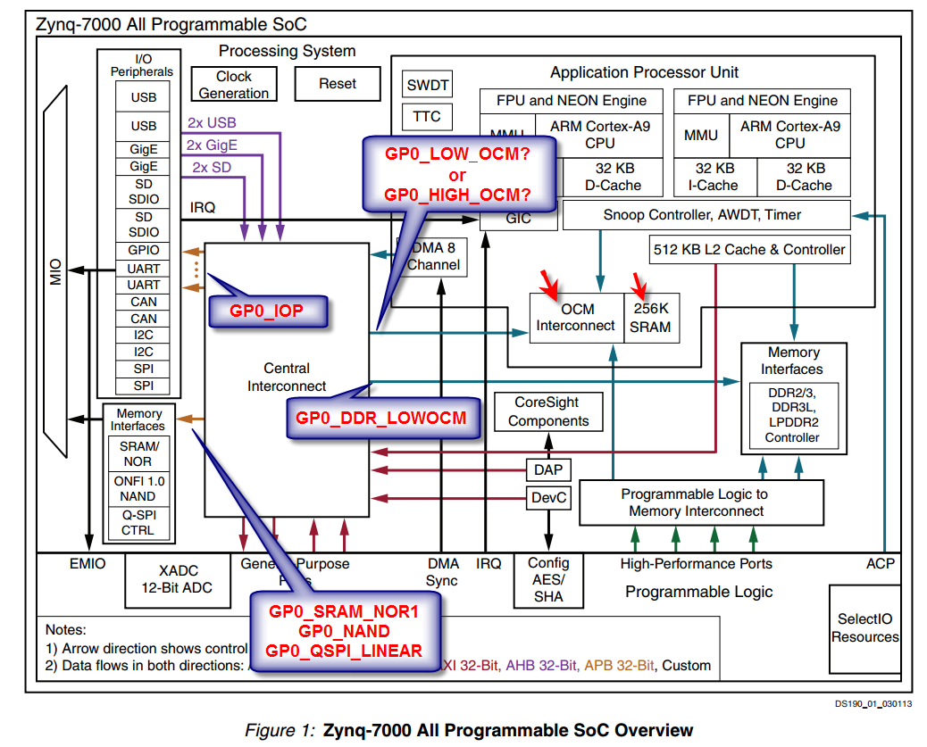
下面我们尝试解读一下,第一幅图时,软件仅仅检测到存在一个AXI Slave接口GP0,当时没有匹配的,所以没有数据,但是当我们加上自行设计的AXI Master接口IP后,软件将二者匹配上了,通过层级结构发现,Zynq上的GP0的Slave接口是匹配用户IP的主机接口的,然后软件自动分配了地址。有一个Base Name,名字是GP0_DDR_LOWOCM,这个名字没看过,不过猜也知道是跟GP0口和DDR相关的,神奇软件怎么知道我想操作DDR呢?猜想应该是配置Zynq时,配置了DDR,所以在Zynq中的总线控制其中激活了DDR相关的段地址,即DDR_LOWCOM。
为了验证上述想法,在Zynq中裁剪掉DDR,具体操作如下:
得到的Zynq封装如下:
可以看到Zynq子系统各种去掉了DDR Control模块,再看Address Editor页面。
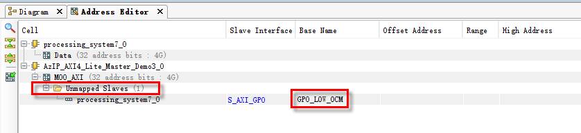
可以看到,由于GP0模块的存在,对于Zynq内部总线接口来说,它配置了一个地址GP0_LOW_OCM,关键词是OCM,经过查询,得知OCM的意思是片上存储器(On-Chip Memory),说白了就是内存映射地址。Zynq内部任何一个可配置的外设硬核,其电路均已经硬件实现了,对应的Zynq内部片地址也是固定的,增加外设,应该就会有新的片内地址。
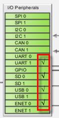
增加了外设USRT1,SD0,USB0,ENET0,QUARD SPI,注意此时没有激活DDR Controller模块。先来看看Zynq的封装。
再来看Address Editor页面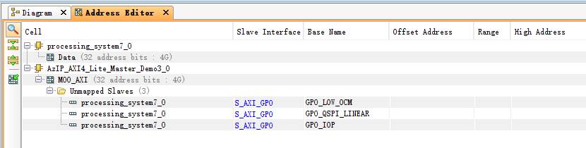
可以看到,对于Quard SPI模块,有单独的地址映射GP0_QSPI_LINEAR,而USRT1,SD0,USB0,ENET0等外设没有,根据Zynq的结构图,大胆猜测,USRT1,SD0,USB0,ENET0等外设均包含在IO Peripherals模块内,因此它们的统一片内地址映射(OCM)的基地址均为GP0_IOP,其中IOP应该就是IO Peripherals的简写。
开始这些数据都没有分配地址,但是前面说了,Zynq中,由于硬件结构都是固定的,剪裁操作是指不激活某些功能模块,个人猜测目的可能是为了低功耗,但是对应的功能模块的内存地址映射都是固定的,跟用户设计的SoC工程无关。
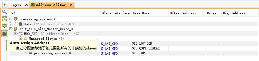
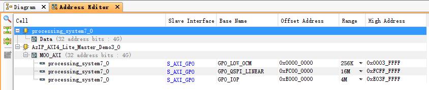
所以这些Zynq内部的映射应该是固定的,我们怎么能够看到呢?点击Address Editor中的Auto Assign Address按钮,如下图所示,系统就会自动填写响应内存映射的Offset Address和Range了。这些都应该是经由GP0路由到这些外设硬核的映射地址。
【补充】LOW_OCM应该就是低速(低性能)存储器地址。有低速对应的肯定就有高速。如下所示。
勾选上图所示项,应该能够打开HIGH_OCM
从上文看出,对于GP0_QSPI_LINEAR和GP0_IOP的命名并没有LOW和OCM等信息。Zynq外设配置不变,仅仅是勾选上图Allow Access to High OCM项,地址映射数据如下。其中HIGH_OCM应该是个独立的内存区域。
去除USRT1,SD0,USB0,ENET0,QUARD SPI等外设,启动DDR Control,仍然勾选Allow Access to High OCM项,得到的Zynq封装如下图:
对应的Address Editor页面如下:
可以看出DDR还是属于LOW_OCM,而HIGH_OCM应该是Zynq系统中的一个特殊区域,具体在哪还不确定,因为跟DDR无关,这里暂时就不关注了。
由于PL中的IP核对Zynq管理的DDR操作是通过地址进行的,因此我们需要对DDR的内存映射整明白。下面再研究研究。
GP0_LOW_OCM已经没有了,但是其对应的地址被包含在GP0_DDR_LOWOCM地址段的低位区间上。
回想《笔记3:PS读写DDR3存储》中的内存映射:
对应的片外DDR3存储芯片的地址的起始位为0x00100000,和这个有点意思。
当然,Address Editor页面中的Offset Address参数和Range参数是可以修改的,而High Address参数是根据前两个参数计算出来的。
必须对Zynq子系统的内存映射原理特别明白,才能正确修改这些参数,因此我们在深入研究研究,看看能不能整明白。
为了深度研究这个问题,在Xilinx Documentation Navigator中搜索OCM,得到如下信息。
可以看到OCM还分为指令OCM和数据OCM。但是这些文件都是比较老的,不是针对Zynq芯片的。没有收获。
上图这些文件也没用,这些讲到都是在PL端用HDL编码实现一个与DDR直接向量的接口控制器的使用方案,而不是设计到Zynq的地址映射方案。
换个思路,查询Zynq的技术文档。

在该文档中得到一些信息,先摘录如下:
Zynq内部有256KB的RAM,就是前面GP0_LOW_OCM或者GP0_HIGH_OCM映射的吗?这个有意思,一定想办法找到。因为之前实验中C语言程序可能就运行在这个内存空间中。
这是前文提到的I/O Peripherals中的内容。
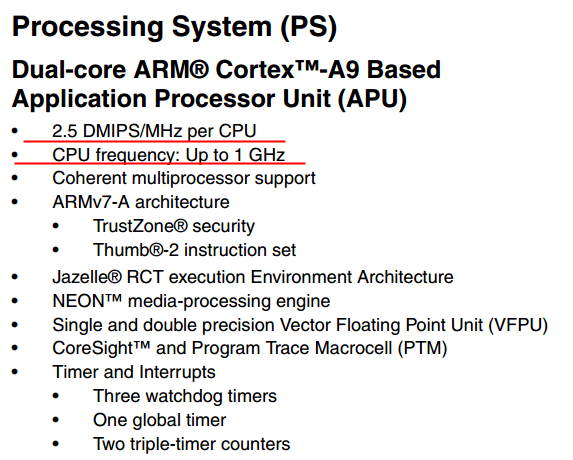
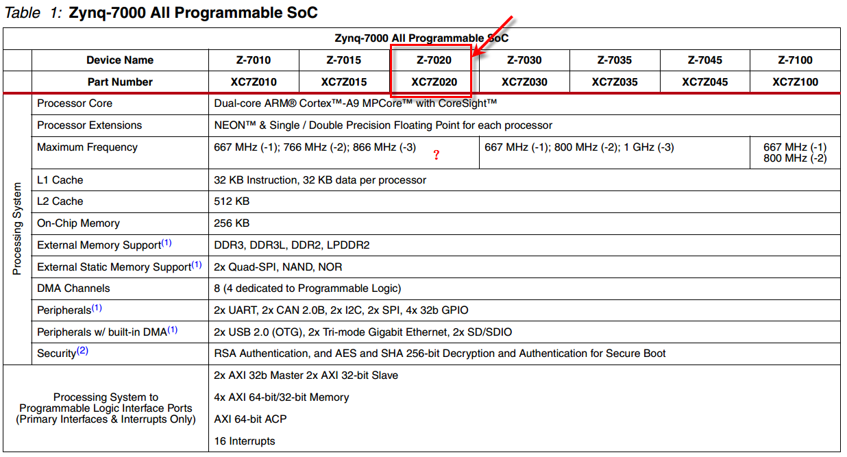
ZedBoard板子用到的芯片是XC7Z020,封装为clg484,但是由于芯片上覆盖了个散热片,不知道是-?。有空问问供货商。
难道是-1???可怜啊,CPU主频最高为667MHz。上图应该是从配置文件中获得的,硬件具体是-?其实还是从芯片丝印看最可靠。不过应该差别不会太大,毕竟是通用开发板,不是为了最求性能的。
下面图很重要!
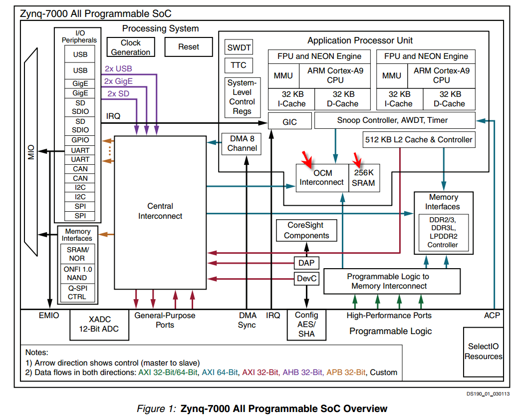
250KB的RAM(OCM)在图中箭头处。
我的猜测,前面出现的内存映射Base Name,应该指的是Central Interconnect的出口,示意图如下:
找到了,就是在这篇文档中,有下列信息:
从上图看到,0x0000_0000是DDR and OCM,
0xFFFC_0000是OCM
那么Zynq内的256KB RAM(OCM)到底怎么访问呢????郁闷
最后的DDR内存映射配置按照系统默认的,如下:
记得主机模块开发是,使用的默认起始地址是0x4000_0000,这个在代码中定义的。不过利用IP核的GUI也能看到。
从前文知道,这个地址是向PL AXI Slave Port #0,即GP0的,Size是1G。
【问题】PL 中的Master IP向0x4000_0000地址写入数据,经过PL中的AXI Interconnect直连,将会转发给GP0,GP0收到后,怎么在转给DDR呢????
【个人猜测】:传入的地址-0x4000_0000,然后进行路由判断吗?假设是这样的,跑起来看看。
至此,本实验的硬件设计完毕。保存后,退出Block Design页面。
6.封装 & Synthesis
然后记得创建HDL Wrapper,
之后对这个工程进行Run Synthesis。
结果没有error和critical warning。
7.行为仿真
原想对这个包含Zynq的顶层模块进行行为仿真,但是看了一眼端口定义。
跟DDR相关的接口时序我根本没法设定,故此放弃了。
直接下板测试吧。
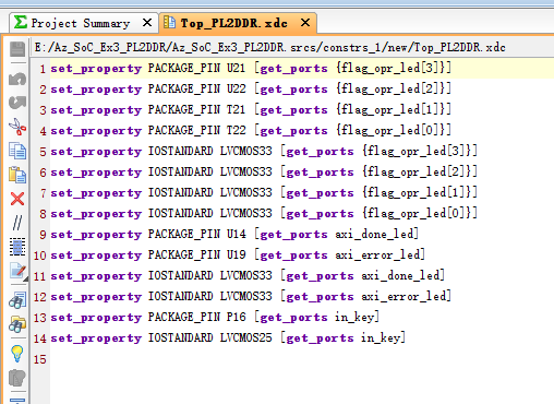
8.管脚绑定
综合完成后,进入Synthesized Design页面,先看看Schematic
然后重点看I/O Planning
根据原理图,PS_CLK(F7)和PS_POR_B(B5)是在Bank500上,驱动电压是3.3V,而PS_RST(C9)是在Bank501上,驱动电压是1.8V。但是这几项是Fixed,改不了,就这样吧。
只能绑定用户管脚,最后的配置图如下:
之后会创建约束文件。
之后,执行Run Implementation和Generate Bitstream。
9.是否还需要启用SDK
直接下板尝试。
没有反应啊。郁闷!Why????
时序逻辑没反应,先检查时钟信号和复位信号,在本实验系统中,PL端的时钟信号和复位信号均是从Zynq子系统中输出的,因此对工程做如下改变,将时钟信号和复位信号引到板上的LED灯处,用于显示和测量。
该工程Synthesis & Implementation后,仍然通过Hardware Manager下载后,现象为FCLK_CLK0驱动的LED灯常亮,使用示波器检测输出为持续高电平,FCLK_RESET0_N驱动的LED灯不亮。根据现象猜测,Zynq子系统中的时钟单元没有正常工作。
原因分析(个人观点):因为Zynq其实是一个ARM系统,其内部的硬核要想按照配置正常工作,应该是在初始化阶段对相应硬核的控制寄存器进行初始化配置,如果是使用Hardware Manager下载是无法操作这一步的。因此尝试使用SDK进行SoC工程配置。
10.是否还需要启用SDK
根据之前的学习,使用SDK有下列几步,不清楚的参看之间的学习笔记。
第一步:Vivado中Export Hardware...(其中需要Include Bitstream)
第二步:Vivado中Launch SDK
第三步:SDK中创建板载支持库函数,Board Support Package
第四步:创建用户工程,Application Project
第五步:编译
第六步:Program FPGA
下面对其中跟本实验有关的进行简单说明
(1)在第三步中,启用SDK可以看到内存映射信息,跟内存相关的一个是DDR,一个是Zynq系统内部的RAM,内存地址如下,根据标题分析,应该是Zynq子系统内部,对于CPU来说的地址设定。
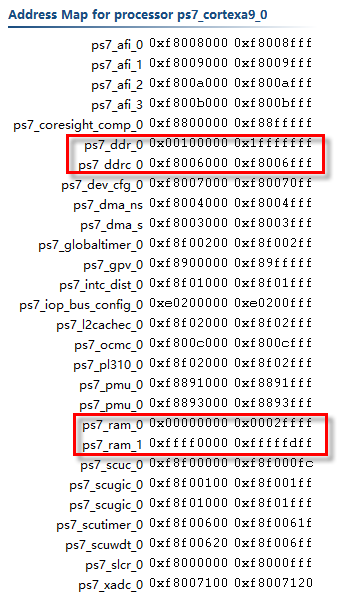
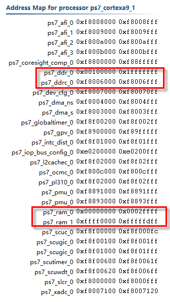
个人猜测:从上图可以看出在Zynq内部,对于两个CPU Core,同一个硬核,操作地址是相同的,从而能够实现双核的数据交互。比如ps7_cortexa9_0能够直接对0x0010_0000的DDR读写数据,同样的ps7_cortexa9_1也可以对该地址的DDR直接读写数据。同时这将会带来一个问题就是同步。另外,还有个问题就是如果是双核运行,每个核都将有自己独立的代码段和栈空间(这两个空间是程序运行时系统使用的,用户不能强行进行读写操作),而堆空间是用户自行申请使用的内存空间,通常用来进行用户数据存储,也就是说堆空间才是双core可以公用的。而无论代码段、栈空间、堆空间的物理载体都是内存(RAM or DDR),因此c语言嵌入式程序对物理内存直接读写时,要避免对代码段和栈空间的地址进行操作。而对代码段和栈空间的配置应该是在编译过程中的link阶段配置的。具体配置接口如下:
这是配置界面,与传统ARM开发对应的配置文件如下所示,相应的详细原理参考传统ARM开发的相关知识。
(2)对Zynq子系统中各个硬核的初始化配置。
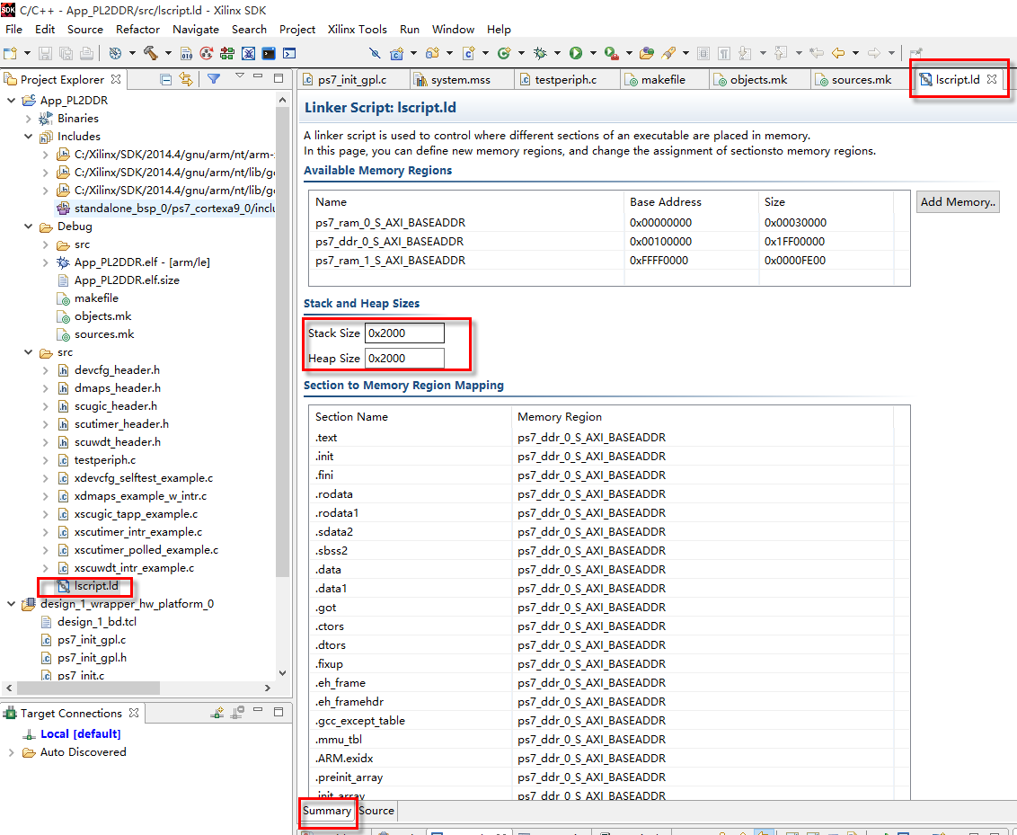
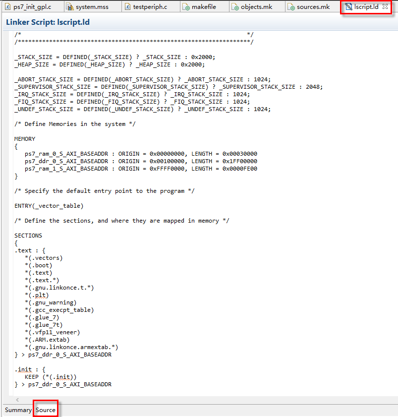
前面分析过,对于Zynq子系统,在不使用CPU Core的架构设计中,如果仅仅使用HardWare下载,Zynq子系统内部的外设硬核也是不能正常工作的。前面分析认为是没有进行初始化配置,在SDK软件中,打开ps7_init.tcl文件如下图所示,从名字可以看出,这是一个初始化的脚本配置文件,既然是tcl文件,应该就不需要c语言调用,而是直接配置,下面截图可以看出是对PLL硬核,Clock硬核、DDR硬核控制寄存器的初始化配置。
其中猜测:mask_write 0XF8000008 0x0000FFFF 0x0000DF0D
应该表示的是向0xF800_0008地址写入数据0x0000_ffff_0000_df0f(共计32bits)
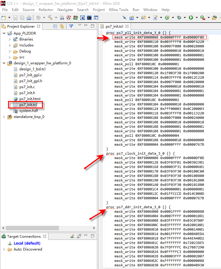
在Run时,SDK软件会在配置“Run ps7_init”项对应的逻辑状态下自动调用该tcl文件完成初始化操作的。
(3)在第四步创建用户工程(Application Project)时,如果还按照之前的经验选择“Hello World”,将会显示如下信息:
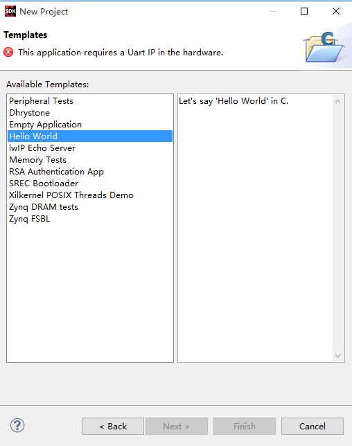
提示信息为:目前硬件项目设计中没有Uart外设硬核,因此该示例不能创建,真丢本实验,仅有Peripheral Tests和Empty Application两项可以使用。经过验证,利用这两个模版都可以实现实验要求,这里只介绍Empty Application模版
使用Empty Application模版,创建的工程如下所示:
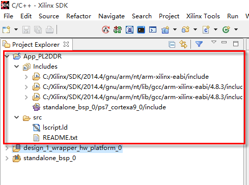
可以看出并没有任何c语言文件。
在src中创建一个c语言文件main.c(文件名可以随便起),其中自行输入一个main函数(必须是这个函数名),保存后,SDK会自动编译,生成一个debug文件和binaries项。
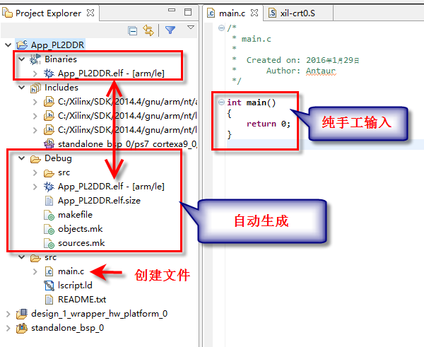
可以看出,这里main函数里什么都没有做。
【补充】对内存分配的进一步分析研究
双击Binaries下的elf文件,显示如下信息:
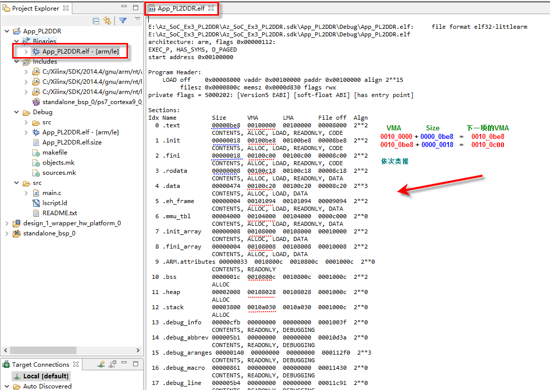
可以看出,编译完成之后,编译软件对嵌入式程序进行的内存划分。而且系统空间大小地址都分配在ddr的低地址区间,因本实验测试时,选用的DDR地址空间应以高地址空间为宜。
在详细分析elf文件中对内存的划分,重点看下图部分。
编译软件分析完毕后,得到的栈空间其实地址为0010_a030,栈空间大小为0000_3800(14K Bytes)。(0010_a030+0000_3800=0010_d830)
c语言嵌入式软件中,如果不是直接地址操作,本实验编译后的软件使用的数据空间为:0010_0000~0010_d830,空间大小为:54.046875K Bytes。
因此,本实验中对DDR的内存读写测试,测试的内存地址区间从0020_0000开始为宜。
另外前文分析时说过,板载DDR为512MB,但是在vivado生成的system.hdf文件中,定义的ps7_ddr_0的内存空间范围只有511MB,少了1MB,当时不知道这1MB时怎么被贪污的。
【个人猜测】但是再看elf文件,可以看到0000_0000开始的空间,是用来进行Debug调试的,因此被Vivado+SDK系统给扣下了,对用户不可见。
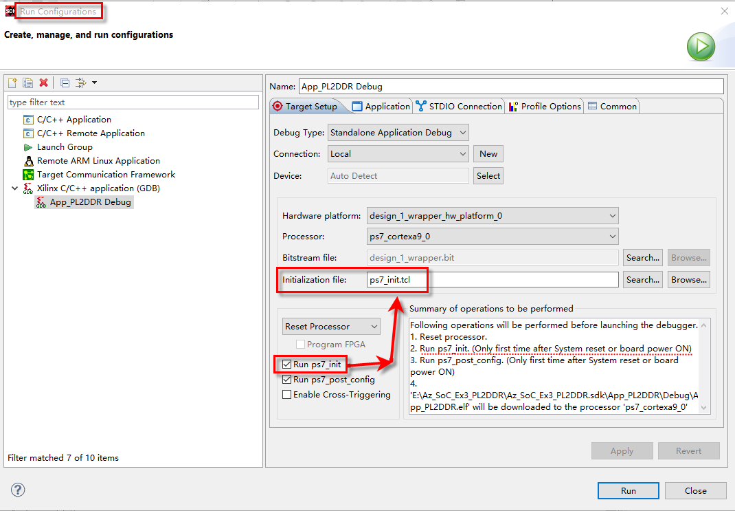
创建完用户逻辑后,配置Run As...项,用于下载程序。
其中,Run Configurations页面前面已经见过很多次,这次重点说明的地方已经框出:
其中“Reset Processor”仅仅时重新下载C语言嵌入式程序,download to processor
当选中“Reset Entire System”项,会先下载PL端的bit文件,然后再下载C语言嵌入式程序,download to processor。
具体说明如下所示。
选择reset processor项后,run成功,SDK Log窗口显示如下信息,可以看出,先执行ps_init.tcl脚本,配置PS的硬核,在运行ps7_post_config(具体工作内容还没整明白),然后复位ps7_cortexa9_0(是的c语言程序从main函数开始运行)。
在开发板上,程序下载成功后,如果按BTN6(PROG),相当于Program FPGA这一项需要重做。因此开发板不再有反应。
在开发板上,程序下载成功后,如果按BTN9(PS-RST),相当于zynq子系统复位,而非CPU(ps7_cortexa9_0)复位,此时需要重新执行Run ps7_init这一项。因此开发板不再有反应。
【结果】下载成功后,开发板反应如设计所示。实验结果表明:
当设置PL端的Master设备访问的地址为0x4020_0000(0x4000_0000为32b GP AXI Slave Port的地址 + 0x0020_0000为DDR内的地址)时,下板运行结果表明内存读写操作是失败的。
当设置PL端的Master设备访问的地址为0x0020_0000(为Zynq子系统内CPU对DDR访问的地址段)时,下板运行结果表明内存读写操作是成功的。
【结论】:
1. 只要SoC系统中,用到了Zynq子系统,无论逻辑上是否激活CPU,都需要使用SDK进行下载,原因时初始化Zynq子系统中硬核。
2. PL端对Zynq子系统中的寄存器进行操作,不需要考虑进行二次内存封装,直接使用Zynq内设定的地址即可。即整个芯片PL+PS是采用统一地址映射的。
【后继】
本实验的最初需求设计,只能保证PL端的Master IP核对Zynq子系统中的内存地址空间读写是正确的,而不能保证一定是读写到了DDR,因此下一个实验,计划利用PL端的Master IP核向0x0020_0000起始的地址端空间写入数据,而用CPU从相应的地址读取数据,进而验证上述结论第二条是否真的是那样的。
附录1:主机IP核底层模块代码
`timescale 1 ns / 1 ps
module AzIP_AXI_Master_3_v1_0_M00_AXI #
(
// Users to add parameters here
// User parameters ends
// Do not modify the parameters beyond this line
// The master will start generating data from the C_M_START_DATA_VALUE value
parameter C_M_START_DATA_VALUE = 32'hAA000000,
// The master requires a target slave base address.
// The master will initiate read and write transactions on the slave with base address specified here as a parameter.
parameter C_M_TARGET_SLAVE_BASE_ADDR = 32'h40000000,
// Width of M_AXI address bus.
// The master generates the read and write addresses of width specified as C_M_AXI_ADDR_WIDTH.
parameter integer C_M_AXI_ADDR_WIDTH = 32,
// Width of M_AXI data bus.
// The master issues write data and accept read data where the width of the data bus is C_M_AXI_DATA_WIDTH
parameter integer C_M_AXI_DATA_WIDTH = 32,
// Transaction number is the number of write
// and read transactions the master will perform as a part of this example memory test.
parameter integer C_M_TRANSACTIONS_NUM = 4
)
(
// Users to add ports here
output reg [3:0] flag_opr, // 输出每次写读操作的对比结果,正确输出高电平
// User ports ends
// Do not modify the ports beyond this line
// Initiate AXI transactions
input wire INIT_AXI_TXN,
// Asserts when ERROR is detected
output reg ERROR,
// Asserts when AXI transactions is complete
output wire TXN_DONE,
// AXI clock signal
input wire M_AXI_ACLK,
// AXI active low reset signal
input wire M_AXI_ARESETN,
// Master Interface Write Address Channel ports. Write address (issued by master)
output wire [C_M_AXI_ADDR_WIDTH-1 : 0] M_AXI_AWADDR,
// Write channel Protection type.
// This signal indicates the privilege and security level of the transaction,
// and whether the transaction is a data access or an instruction access.
output wire [2 : 0] M_AXI_AWPROT,
// Write address valid.
// This signal indicates that the master signaling valid write address and control information.
output wire M_AXI_AWVALID,
// Write address ready.
// This signal indicates that the slave is ready to accept an address and associated control signals.
input wire M_AXI_AWREADY,
// Master Interface Write Data Channel ports. Write data (issued by master)
output wire [C_M_AXI_DATA_WIDTH-1 : 0] M_AXI_WDATA,
// Write strobes.
// This signal indicates which byte lanes hold valid data.
// There is one write strobe bit for each eight bits of the write data bus.
output wire [C_M_AXI_DATA_WIDTH/8-1 : 0] M_AXI_WSTRB,
// Write valid. This signal indicates that valid write data and strobes are available.
output wire M_AXI_WVALID,
// Write ready. This signal indicates that the slave can accept the write data.
input wire M_AXI_WREADY,
// Master Interface Write Response Channel ports.
// This signal indicates the status of the write transaction.
input wire [1 : 0] M_AXI_BRESP,
// Write response valid.
// This signal indicates that the channel is signaling a valid write response
input wire M_AXI_BVALID,
// Response ready. This signal indicates that the master can accept a write response.
output wire M_AXI_BREADY,
// Master Interface Read Address Channel ports. Read address (issued by master)
output wire [C_M_AXI_ADDR_WIDTH-1 : 0] M_AXI_ARADDR,
// Protection type.
// This signal indicates the privilege and security level of the transaction,
// and whether the transaction is a data access or an instruction access.
output wire [2 : 0] M_AXI_ARPROT,
// Read address valid.
// This signal indicates that the channel is signaling valid read address and control information.
output wire M_AXI_ARVALID,
// Read address ready.
// This signal indicates that the slave is ready to accept an address and associated control signals.
input wire M_AXI_ARREADY,
// Master Interface Read Data Channel ports. Read data (issued by slave)
input wire [C_M_AXI_DATA_WIDTH-1 : 0] M_AXI_RDATA,
// Read response. This signal indicates the status of the read transfer.
input wire [1 : 0] M_AXI_RRESP,
// Read valid. This signal indicates that the channel is signaling the required read data.
input wire M_AXI_RVALID,
// Read ready. This signal indicates that the master can accept the read data and response information.
output wire M_AXI_RREADY
);
// function called clogb2 that returns an integer which has the
// value of the ceiling of the log base 2
function integer clogb2 (input integer bit_depth);
begin
for(clogb2=0; bit_depth>0; clogb2=clogb2+1)
bit_depth = bit_depth >> 1;
end
endfunction
// TRANS_NUM_BITS is the width of the index counter for
// number of write or read transaction.
localparam integer TRANS_NUM_BITS = clogb2(C_M_TRANSACTIONS_NUM-1);
// Example State machine to initialize counter, initialize write transactions,
// initialize read transactions and comparison of read data with the
// written data words.
parameter [1:0] IDLE = 2'b00, // This state initiates AXI4Lite transaction
// after the state machine changes state to INIT_WRITE
// when there is 0 to 1 transition on INIT_AXI_TXN
INIT_WRITE = 2'b01, // This state initializes write transaction,
// once writes are done, the state machine
// changes state to INIT_READ
INIT_READ = 2'b10, // This state initializes read transaction
// once reads are done, the state machine
// changes state to INIT_COMPARE
INIT_COMPARE = 2'b11; // This state issues the status of comparison
// of the written data with the read data
reg [1:0] mst_exec_state;
// AXI4LITE signals
//write address valid
reg axi_awvalid;
//write data valid
reg axi_wvalid;
//read address valid
reg axi_arvalid;
//read data acceptance
reg axi_rready;
//write response acceptance
reg axi_bready;
//write address
reg [C_M_AXI_ADDR_WIDTH-1 : 0] axi_awaddr;
//write data
reg [C_M_AXI_DATA_WIDTH-1 : 0] axi_wdata;
//read addresss
reg [C_M_AXI_ADDR_WIDTH-1 : 0] axi_araddr;
//Asserts when there is a write response error
wire write_resp_error;
//Asserts when there is a read response error
wire read_resp_error;
//A pulse to initiate a write transaction
reg start_single_write;
//A pulse to initiate a read transaction
reg start_single_read;
//Asserts when a single beat write transaction is issued and remains asserted till the completion of write trasaction.
reg write_issued;
//Asserts when a single beat read transaction is issued and remains asserted till the completion of read trasaction.
reg read_issued;
//flag that marks the completion of write trasactions. The number of write transaction is user selected by the parameter C_M_TRANSACTIONS_NUM.
reg writes_done;
//flag that marks the completion of read trasactions. The number of read transaction is user selected by the parameter C_M_TRANSACTIONS_NUM
reg reads_done;
//The error register is asserted when any of the write response error, read response error or the data mismatch flags are asserted.
reg error_reg;
//index counter to track the number of write transaction issued
reg [TRANS_NUM_BITS : 0] write_index;
//index counter to track the number of read transaction issued
reg [TRANS_NUM_BITS : 0] read_index;
//Expected read data used to compare with the read data.
reg [C_M_AXI_DATA_WIDTH-1 : 0] expected_rdata;
//Flag marks the completion of comparison of the read data with the expected read data
reg compare_done;
//This flag is asserted when there is a mismatch of the read data with the expected read data.
reg read_mismatch;
//Flag is asserted when the write index reaches the last write transction number
reg last_write;
//Flag is asserted when the read index reaches the last read transction number
reg last_read;
reg init_txn_ff;
reg init_txn_ff2;
reg init_txn_edge;
wire init_txn_pulse;
reg [7:0] rs_test_data_w_count; // 写入数据递增计数器
reg [7:0] rs_test_data_c_count; // 数据对比计数器
reg r_flag;
// I/O Connections assignments
//Adding the offset address to the base addr of the slave
assign M_AXI_AWADDR = C_M_TARGET_SLAVE_BASE_ADDR + axi_awaddr;
//AXI 4 write data
assign M_AXI_WDATA = axi_wdata;
assign M_AXI_AWPROT = 3'b000;
assign M_AXI_AWVALID = axi_awvalid;
//Write Data(W)
assign M_AXI_WVALID = axi_wvalid;
//Set all byte strobes in this example
assign M_AXI_WSTRB = 4'b1111;
//Write Response (B)
assign M_AXI_BREADY = axi_bready;
//Read Address (AR)
assign M_AXI_ARADDR = C_M_TARGET_SLAVE_BASE_ADDR + axi_araddr;
assign M_AXI_ARVALID = axi_arvalid;
assign M_AXI_ARPROT = 3'b001;
//Read and Read Response (R)
assign M_AXI_RREADY = axi_rready;
//Example design I/O
assign TXN_DONE = compare_done;
assign init_txn_pulse = (!init_txn_ff2) && init_txn_ff; //原代码时上升沿触发
//Generate a pulse to initiate AXI transaction.
always @(posedge M_AXI_ACLK)
begin
// Initiates AXI transaction delay
if (M_AXI_ARESETN == 0 )
begin
init_txn_ff <= 1'b0;
init_txn_ff2 <= 1'b0;
end
else
begin
init_txn_ff <= INIT_AXI_TXN;
init_txn_ff2 <= init_txn_ff;
end
end
//--------------------
//Write Address Channel
//--------------------
// The purpose of the write address channel is to request the address and
// command information for the entire transaction. It is a single beat
// of information.
// Note for this example the axi_awvalid/axi_wvalid are asserted at the same
// time, and then each is deasserted independent from each other.
// This is a lower-performance, but simplier control scheme.
// AXI VALID signals must be held active until accepted by the partner.
// A data transfer is accepted by the slave when a master has
// VALID data and the slave acknoledges it is also READY. While the master
// is allowed to generated multiple, back-to-back requests by not
// deasserting VALID, this design will add rest cycle for
// simplicity.
// Since only one outstanding transaction is issued by the user design,
// there will not be a collision between a new request and an accepted
// request on the same clock cycle.
always @(posedge M_AXI_ACLK)
begin
//Only VALID signals must be deasserted during reset per AXI spec
//Consider inverting then registering active-low reset for higher fmax
if (M_AXI_ARESETN == 0 || init_txn_pulse == 1'b1)
begin
axi_awvalid <= 1'b0;
end
//Signal a new address/data command is available by user logic
else
begin
if (start_single_write)
begin
axi_awvalid <= 1'b1;
end
//Address accepted by interconnect/slave (issue of M_AXI_AWREADY by slave)
else if (M_AXI_AWREADY && axi_awvalid)
begin
axi_awvalid <= 1'b0;
end
end
end
// start_single_write triggers a new write
// transaction. write_index is a counter to
// keep track with number of write transaction
// issued/initiated
always @(posedge M_AXI_ACLK)
begin
if (M_AXI_ARESETN == 0 || init_txn_pulse == 1'b1)
begin
write_index <= 0;
if (M_AXI_ARESETN == 0) begin
rs_test_data_w_count <= 8'h00;
end
else if (init_txn_pulse == 1'b1) begin
rs_test_data_w_count <= rs_test_data_w_count;
end
end
// Signals a new write address/ write data is
// available by user logic
else if (start_single_write)
begin
write_index <= write_index + 1;
rs_test_data_w_count <= rs_test_data_w_count+1;
end
end
//--------------------
//Write Data Channel
//--------------------
//The write data channel is for transfering the actual data.
//The data generation is speific to the example design, and
//so only the WVALID/WREADY handshake is shown here
always @(posedge M_AXI_ACLK)
begin
if (M_AXI_ARESETN == 0 || init_txn_pulse == 1'b1)
begin
axi_wvalid <= 1'b0;
end
//Signal a new address/data command is available by user logic
else if (start_single_write)
begin
axi_wvalid <= 1'b1;
end
//Data accepted by interconnect/slave (issue of M_AXI_WREADY by slave)
else if (M_AXI_WREADY && axi_wvalid)
begin
axi_wvalid <= 1'b0;
end
end
//----------------------------
//Write Response (B) Channel
//----------------------------
//The write response channel provides feedback that the write has committed
//to memory. BREADY will occur after both the data and the write address
//has arrived and been accepted by the slave, and can guarantee that no
//other accesses launched afterwards will be able to be reordered before it.
//The BRESP bit [1] is used indicate any errors from the interconnect or
//slave for the entire write burst. This example will capture the error.
//While not necessary per spec, it is advisable to reset READY signals in
//case of differing reset latencies between master/slave.
always @(posedge M_AXI_ACLK)
begin
if (M_AXI_ARESETN == 0 || init_txn_pulse == 1'b1)
begin
axi_bready <= 1'b0;
end
// accept/acknowledge bresp with axi_bready by the master
// when M_AXI_BVALID is asserted by slave
else if (M_AXI_BVALID && ~axi_bready)
begin
axi_bready <= 1'b1;
end
// deassert after one clock cycle
else if (axi_bready)
begin
axi_bready <= 1'b0;
end
// retain the previous value
else
axi_bready <= axi_bready;
end
//Flag write errors
assign write_resp_error = (axi_bready & M_AXI_BVALID & M_AXI_BRESP[1]);
//----------------------------
//Read Address Channel
//----------------------------
//start_single_read triggers a new read transaction. read_index is a counter to
//keep track with number of read transaction issued/initiated
always @(posedge M_AXI_ACLK)
begin
if (M_AXI_ARESETN == 0 || init_txn_pulse == 1'b1)
begin
read_index <= 0;
if (M_AXI_ARESETN == 0) begin
rs_test_data_c_count <= 8'h00;
end
else if (init_txn_pulse == 1'b1) begin
rs_test_data_c_count <= rs_test_data_c_count;
end
end
// Signals a new read address is
// available by user logic
else if (start_single_read)
begin
read_index <= read_index + 1;
rs_test_data_c_count <= rs_test_data_c_count+1;
end
end
// A new axi_arvalid is asserted when there is a valid read address
// available by the master. start_single_read triggers a new read
// transaction
always @(posedge M_AXI_ACLK)
begin
if (M_AXI_ARESETN == 0 || init_txn_pulse == 1'b1)
begin
axi_arvalid <= 1'b0;
end
//Signal a new read address command is available by user logic
else if (start_single_read)
begin
axi_arvalid <= 1'b1;
end
//RAddress accepted by interconnect/slave (issue of M_AXI_ARREADY by slave)
else if (M_AXI_ARREADY && axi_arvalid)
begin
axi_arvalid <= 1'b0;
end
// retain the previous value
end
//--------------------------------
//Read Data (and Response) Channel
//--------------------------------
//The Read Data channel returns the results of the read request
//The master will accept the read data by asserting axi_rready
//when there is a valid read data available.
//While not necessary per spec, it is advisable to reset READY signals in
//case of differing reset latencies between master/slave.
always @(posedge M_AXI_ACLK)
begin
if (M_AXI_ARESETN == 0 || init_txn_pulse == 1'b1)
begin
axi_rready <= 1'b0;
end
// accept/acknowledge rdata/rresp with axi_rready by the master
// when M_AXI_RVALID is asserted by slave
else if (M_AXI_RVALID && ~axi_rready)
begin
axi_rready <= 1'b1;
end
// deassert after one clock cycle
else if (axi_rready)
begin
axi_rready <= 1'b0;
end
// retain the previous value
end
//Flag write errors
assign read_resp_error = (axi_rready & M_AXI_RVALID & M_AXI_RRESP[1]);
//--------------------------------
//User Logic
//--------------------------------
//Address/Data Stimulus
//Address/data pairs for this example. The read and write values should
//match.
//Modify these as desired for different address patterns.
//Write Addresses
always @(posedge M_AXI_ACLK)
begin
if (M_AXI_ARESETN == 0 || init_txn_pulse == 1'b1)
begin
if (M_AXI_ARESETN == 0) begin
axi_awaddr <= 0;
end
else if (init_txn_pulse == 1'b1) begin
axi_awaddr <= axi_awaddr;
end
end
// Signals a new write address/ write data is
// available by user logic
else if (M_AXI_AWREADY && axi_awvalid)
begin
axi_awaddr <= axi_awaddr + 32'h00000004;
end
end
// Write data generation
always @(posedge M_AXI_ACLK)
begin
if (M_AXI_ARESETN == 0 || init_txn_pulse == 1'b1 )
begin
if (M_AXI_ARESETN == 0) begin
axi_wdata <= C_M_START_DATA_VALUE;
end
else if (init_txn_pulse == 1'b1) begin
axi_wdata <= axi_wdata;
end
end
// Signals a new write address/ write data is
// available by user logic
else if (M_AXI_WREADY && axi_wvalid)
begin
axi_wdata <= C_M_START_DATA_VALUE + rs_test_data_w_count;
end
end
//Read Addresses
always @(posedge M_AXI_ACLK)
begin
if (M_AXI_ARESETN == 0 || init_txn_pulse == 1'b1)
begin
if (M_AXI_ARESETN == 0) begin
axi_araddr <= 0;
end
else if (init_txn_pulse == 1'b1) begin
axi_araddr <= axi_araddr;
end
end
// Signals a new write address/ write data is
// available by user logic
else if (M_AXI_ARREADY && axi_arvalid)
begin
axi_araddr <= axi_araddr + 32'h00000004;
end
end
always @(posedge M_AXI_ACLK)
begin
if (M_AXI_ARESETN == 0 || init_txn_pulse == 1'b1)
begin
if (M_AXI_ARESETN == 0) begin
expected_rdata <= C_M_START_DATA_VALUE;
end
else if (init_txn_pulse == 1'b1) begin
expected_rdata <= expected_rdata;
end
end
// Signals a new write address/ write data is
// available by user logic
else if (M_AXI_RVALID && axi_rready)
begin
expected_rdata <= C_M_START_DATA_VALUE + rs_test_data_c_count;
end
end
//implement master command interface state machine
always @ ( posedge M_AXI_ACLK)
begin
if (M_AXI_ARESETN == 1'b0)
begin
// reset condition
// All the signals are assigned default values under reset condition
mst_exec_state <= IDLE;
start_single_write <= 1'b0;
write_issued <= 1'b0;
start_single_read <= 1'b0;
read_issued <= 1'b0;
compare_done <= 1'b0;
ERROR <= 1'b0;
end
else
begin
// state transition
case (mst_exec_state)
IDLE:
// This state is responsible to initiate
// AXI transaction when init_txn_pulse is asserted
if ( init_txn_pulse == 1'b1 )
begin
mst_exec_state <= INIT_WRITE;
ERROR <= 1'b0;
compare_done <= 1'b0;
end
else
begin
mst_exec_state <= IDLE;
end
INIT_WRITE:
// This state is responsible to issue start_single_write pulse to
// initiate a write transaction. Write transactions will be
// issued until last_write signal is asserted.
// write controller
if (writes_done)
begin
mst_exec_state <= INIT_READ;//
end
else
begin
mst_exec_state <= INIT_WRITE;
if (~axi_awvalid && ~axi_wvalid && ~M_AXI_BVALID && ~last_write && ~start_single_write && ~write_issued)
begin
start_single_write <= 1'b1;
write_issued <= 1'b1;
end
else if (axi_bready)
begin
write_issued <= 1'b0;
end
else
begin
start_single_write <= 1'b0; //Negate to generate a pulse
end
end
INIT_READ:
// This state is responsible to issue start_single_read pulse to
// initiate a read transaction. Read transactions will be
// issued until last_read signal is asserted.
// read controller
if (reads_done)
begin
mst_exec_state <= INIT_COMPARE;
end
else
begin
mst_exec_state <= INIT_READ;
if (~axi_arvalid && ~M_AXI_RVALID && ~last_read && ~start_single_read && ~read_issued)
begin
start_single_read <= 1'b1;
read_issued <= 1'b1;
end
else if (axi_rready)
begin
read_issued <= 1'b0;
end
else
begin
start_single_read <= 1'b0; //Negate to generate a pulse
end
end
INIT_COMPARE:
begin
// This state is responsible to issue the state of comparison
// of written data with the read data. If no error flags are set,
// compare_done signal will be asseted to indicate success.
ERROR <= error_reg;
mst_exec_state <= IDLE;
compare_done <= 1'b1;
end
default :
begin
mst_exec_state <= IDLE;
end
endcase
end
end //MASTER_EXECUTION_PROC
//Terminal write count
always @(posedge M_AXI_ACLK)
begin
if (M_AXI_ARESETN == 0 || init_txn_pulse == 1'b1)
last_write <= 1'b0;
//The last write should be associated with a write address ready response
else if ((write_index == C_M_TRANSACTIONS_NUM) && M_AXI_AWREADY)
last_write <= 1'b1;
else
last_write <= last_write;
end
//Check for last write completion.
//This logic is to qualify the last write count with the final write
//response. This demonstrates how to confirm that a write has been
//committed.
always @(posedge M_AXI_ACLK)
begin
if (M_AXI_ARESETN == 0 || init_txn_pulse == 1'b1)
writes_done <= 1'b0;
//The writes_done should be associated with a bready response
else if (last_write && M_AXI_BVALID && axi_bready)
writes_done <= 1'b1;
else
writes_done <= writes_done;
end
//------------------
//Read example
//------------------
//Terminal Read Count
always @(posedge M_AXI_ACLK)
begin
if (M_AXI_ARESETN == 0 || init_txn_pulse == 1'b1)
last_read <= 1'b0;
//The last read should be associated with a read address ready response
else if ((read_index == C_M_TRANSACTIONS_NUM) && (M_AXI_ARREADY) )
last_read <= 1'b1;
else
last_read <= last_read;
end
/*
Check for last read completion.
This logic is to qualify the last read count with the final read
response/data.
*/
always @(posedge M_AXI_ACLK)
begin
if (M_AXI_ARESETN == 0 || init_txn_pulse == 1'b1)
reads_done <= 1'b0;
//The reads_done should be associated with a read ready response
else if (last_read && M_AXI_RVALID && axi_rready)
reads_done <= 1'b1;
else
reads_done <= reads_done;
end
//-----------------------------
//Example design error register
//-----------------------------
//Data Comparison
always @(posedge M_AXI_ACLK)
begin
if (M_AXI_ARESETN == 0 || INIT_AXI_TXN == 1'b0) begin
read_mismatch <= 1'b0;
flag_opr <= 4'h0;
r_flag <= 1'b0;
end
//The read data when available (on axi_rready) is compared with the expected data
else if (M_AXI_RVALID && axi_rready) begin
r_flag <= 1'b1;
if (M_AXI_RDATA != expected_rdata) begin
read_mismatch <= 1'b1;
case (read_index-1)
2'b00: flag_opr[0] <= 1'b0;
2'b01: flag_opr[1] <= 1'b0;
2'b10: flag_opr[2] <= 1'b0;
2'b11: flag_opr[3] <= 1'b0;
endcase
end
else begin
read_mismatch <= read_mismatch;
case (read_index-1)
2'b00: flag_opr[0] <= 1'b1;
2'b01: flag_opr[1] <= 1'b1;
2'b10: flag_opr[2] <= 1'b1;
2'b11: flag_opr[3] <= 1'b1;
endcase
end
end
else begin
r_flag <= 1'b0;
end
end
// Register and hold any data mismatches, or read/write interface errors
always @(posedge M_AXI_ACLK)
begin
if (M_AXI_ARESETN == 0 || init_txn_pulse == 1'b1)
error_reg <= 1'b0;
//Capture any error types
else if (read_mismatch || write_resp_error || read_resp_error)
error_reg <= 1'b1;
else
error_reg <= error_reg;
end
// Add user logic here
// User logic ends
endmodule
附录2:主从机直连测试系统行为仿真文件
`timescale 1ns / 1ps
module Sim_AXI4_Lite_Direct_Connect();
reg axi_ACLK; // AXI总线时钟
reg axi_ARESETn; // 系统复位信号,低电平有效
reg r_app_txn; // 应用级复位信号,负脉冲,上升沿复位
wire w_err; // 状态指示,异常
wire w_txn_done; // 状态指示,发送完毕
wire [3:0] w_flag_opr;
Top_AXI4_Lite_Direct_Connect # (
.C_AXI_START_DATA_VALUE(32'hAA000000),
.C_AXI_TARGET_SLAVE_BASE_ADDR(32'h40000000),
.C_AXI_ADDR_WIDTH(32),
.C_AXI_DATA_WIDTH(32),
.C_AXI_TRANSACTIONS_NUM(4) // 一次触发读写次数,不能大于4
) Ut1 (
.axi_ACLK(axi_ACLK),
.axi_ARESETn(axi_ARESETn),
.app_TXn(r_app_txn),
.state_err(w_err),
.state_done(w_txn_done),
.flag_opr(w_flag_opr)
);
parameter PERIOD = 2;
always begin
#(PERIOD/2);
axi_ACLK = ~axi_ACLK;
end
initial begin
axi_ACLK = 1'b0;
axi_ARESETn = 1'b1;
r_app_txn = 1'b1;
#(4*PERIOD);
axi_ARESETn = 1'b0;
#(1*PERIOD);
r_app_txn = 1'b0;
#(2*PERIOD);
axi_ARESETn = 1'b1;
#(2*PERIOD);
r_app_txn = 1'b1;
#(58*PERIOD);
r_app_txn = 1'b0;
#(3*PERIOD);
r_app_txn = 1'b1;
end
endmodule
FPGA基础知识21(PL控制PS端DDR的设计)相关推荐
- 【ZYNQ Ultrascale+ MPSOC FPGA教程】第三十二章 PL读写PS端DDR数据
本原创教程由芯驿电子科技(上海)有限公司(ALINX)创作,版权归本公司所有,如需转载,需授权并注明出处. 适用于板卡型号: AXU2CGA/AXU2CGB/AXU3EG/AXU4EV-E/AXU4E ...
- ZYNQ的PL控制PS的DDR
本次工程是用PL端控制PS的DDR,下面是一些过程 1. 创建一个ZYNQ核 选择高速互联总线,因为DDR速率比较快,所以PS与PL端的交互,我们选择HP,高速AXI连接,位宽选择32,和DDR位宽保 ...
- zynq开发系列5:通过AXI GPIO的中断实现PL端按键控制PS端LED(SDK开发详解)
axi_gpio是PL端gpio(FPGA资源搭建的软核),ps7_gpio是ps端gpio(硬核).打开Documentation的示例Examples,可知第二个是关于中断的示例.导入示例impo ...
- 初学者必须要知道的FPGA基础知识
初学者必须要知道的FPGA基础知识 一.FPGA是什么? 在<FPGA至简设计原理与应用>一书里是这样描述的:『FPGA的全称为Field-Programmable Gate Array, ...
- FPGA基础知识|芯片设计基础知识
FPGA 基础知识 可查看原文:FPGA基础知识 1.查找表 LUT 和编程方式第一部分: 查找表 LUT FPGA 是在 PAL.GAL.EPLD.CPLD 等可编程器件的基础上进一步发展的产物.它 ...
- FPGA基础知识极简教程(7)详解亚稳态与跨时钟域传输
博文目录 写在前面 正文 FPGA或ASIC中的传播延迟 建立和保持时间是什么? 建立和保持时间与传播延迟和时钟频率有何关系? 如果违反建立和保持时间会发生什么? FPGA中的亚稳定是什么? 亚稳态何 ...
- FPGA基础知识极简教程(4)从FIFO设计讲起之异步FIFO篇
博文目录 写在前面 正文 同步FIFO回顾 $clog2()系统函数使用 综合属性控制资源使用 异步FIFO设计 FIFO用途回顾 异步FIFO原理回顾 异步FIFO设计 异步FIFO仿真 参考资料 ...
- SAP SD基础知识之输出控制(Output Control)
SAP SD基础知识之输出控制(Output Control) 一,销售的输出类型 Output是用于和商业伙伴及系统交换信息的通信方式.我们可以为不同的销售凭证如报价单,订单,交货单,发票设置out ...
- FPGA基础知识极简教程(10)二进制到BCD转换算法
文章目录 写在前面 正文 快速认识 实现方式一 实现方式二 写在最后 写在前面 FPGA基础知识极简教程(9)讲到了七段数码管的显示Verilog设计,我们都知道,要在数码管上显示的数字,使用BCD编 ...
- Java基础知识 21(Set集合,HashSet集合以及它的三种遍历方式(迭代器,增强for循环,forEach),LinkedHashSet集合,TreeSet集合(自然排序法,比较器排序法))
Java基础知识 21 Set集合 Set集合:一个不包含重复元素的Collection集合,元素不重复,List集合是允许元素重复的. Set接口的三个字类:HashSet(),LinkedHash ...
最新文章
- 无法远程分发安装软件原因
- 科大星云诗社动态20210308
- [BZOJ2502]清理雪道解题报告|带下界的最小流
- python可移植性强吗_你真的了解Python吗?本文可以让你更深度了解Python
- Mr.J--代码雨( Matrix)
- 【转】POP3、SMTP和IMAP之间的区别和联系
- 1小时搞懂设计模式之原型模式
- USB 3.1 与 Type-C 接口有什么关系呢
- autolisp获取目录服务器信息失败,大神们,帮忙看看这个代码哪儿有问题?老是出现“参数类型错误:...
- hadoop中MapReduce多种join实现实例分析
- 如何在Vue项目中使用vw实现移动端适配
- java调用vissim的com接口_VISSIM 高级应用COM接口开发初级入门
- 法兰克焊接机器人编程入门_Fanuc ARC MATE 焊接机器人操作编程.pdf
- MQTT测试工具MQTT.FX
- H264解码之PES流解析
- 万用表二极管档位点亮发光二极管LED
- 每天15分钟中度或快步走以燃烧100卡路里的热量
- 笔记本合上盖子怎么不休眠了?
- ASO优化常见的问题精选之ASO指数是什么?
- Nature reviews Neurology:癫痫合并神经行为障碍:基于网络的精确分类