FPGA_DS18B20温度传感器手册介绍以及接口代码编写思路
一. DS18B20大概介绍
1. Power
电源可以用 parasite power 或者 external power,普遍选择外部电源
2. DS18B20内部存储一共有9个字节
(1).DS18B20内部存储框图
读取温度只需要用byte0,byte1
![]()
(2).DS18B20 温度有四种分辨率模式(9,10,11,12bit)
采用12bit分辨率,高5位(S)是判断温度正负(0为正,1为负)
下面两图分别为温度高低字节,温度与读取数据之间的关联
![]()
3.DS18B20采用单总线协议
- All data and commands are transmitted least significant bit first(读写都是从最低位开始) over the 1-Wire bus.
- 1-wire : 异步半双工串行通信
4.DS18B20发送命令顺序
(1). TRANSACTION SEQUENCE
The transaction sequence for accessing the DS18B20 is as follows:
三个顺序必须遵行 (初始化 - ROM命令 - DS18B20命令)
- Step 1. Initialization
- Step 2. ROM Command (followed by any required data exchange)
- Step 3. DS18B20 Function Command (followed by any required data exchange)
It is very important to follow this sequence every time the DS18B20 is accessed, as the DS18B20 will not respond if any steps in the sequence are missing or out of order. Exceptions to this rule are the Search ROM [F0h] and Alarm Search [ECh] commands. After issuing either of these ROM commands, the master must return to Step 1 in the sequence.
(2).ROM,DS18B20命令流程图
读取温度需要的命令:SKIP ROM [CCh] (跳过ROM命令),CONVERT T [44h](温度转换命令),READ SCRATCHPAD [BEh] (温度读取命令)
![]()
DS18B20 函数命令流程表
![]()
二. DS1820 INITIAL(初始化)
INITIALIZATION PROCEDURE: RESET AND PRESENCE PULSES (复位脉冲和存在脉冲)
All communication with the DS18B20 begins with an initialization sequence that consists of a reset pulse from the master followed by a presence pulse from the DS18B20. This is illustrated in Figure 13. When the DS18B20 sends the presence pulse in response to the reset, it is indicating to the master that it is on the bus and ready to operate.
During the initialization sequence the bus master transmits (TX) the reset pulse by pulling the 1-Wire bus low for a minimum of 480us. The bus master then releases the bus and goes into receive mode (RX). When the bus is released, the 5k pullup resistor pulls the 1-Wire bus high. When the DS18B20 detects this rising edge, it waits 15us to 60us and then transmits a presence pulse by pulling the 1-Wire bus low for 60us to 240us
1.初始化过程
- 复位脉冲:控制总线拉低480us以上,然后释放总线
- WAIT:15~60us
- 检测存在脉冲:在60~240us内总线有一个低电平
- wait:1000us-复位脉冲-WAIT-检测存在脉冲
- 初始化完成.
2.初始化时序图
![]()
三.向DS18B20 写命令
WRITE TIME SLOTS
There are two types of write time slots: “Write 1” time slots and “Write 0” time slots. The bus master uses a Write 1 time slot to write a logic 1 to the DS18B20 and a Write 0 time slot to write a logic 0 to the DS18B20. All write time slots must be a minimum of 60us in duration with a minimum of a 1 s recovery time between individual write slots. Both types of write time slots are initiated by the master pulling the 1-Wire bus low (see Figure 14). To generate a Write 1 time slot, after pulling the 1-Wire bus low, the bus master must release the 1-Wire bus within 15us. When the bus is released, the 5k pullup resistor will pull the bus high.
To generate a Write 0 time slot, after pulling the 1-Wire bus low, the bus master must continue to hold the bus low for the duration of the time slot (at least 60us). The DS18B20 samples the 1-Wire bus during a window that lasts from 15us to 60us after the master initiates the write time slot. If the bus is high during the sampling window, a 1 is written to the DS18B20. If the line is low, a 0 is written to the DS18B20.
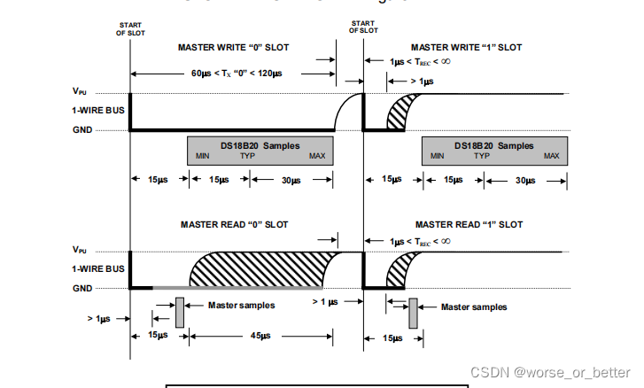
1.写时序图
![]()
2.写过程
1.写0缝隙:控制总线拉低60120us,然后释放总线(dq会在1545us之间采样)
.写1缝隙:控制总线拉低15us以内,然后ds18b20释放总线(dq会在15~45us之间采样)
2.wait:每一次写完1bit都需要等待1us以上
3.写完成,根据需求判断是否需要读取下个bit
四.读取DS18B20数据
READ TIME SLOTS
The DS18B20 can only transmit data to the master when the master issues read time slots. Therefore, the master must generate read time slots immediately after issuing a Read Scratchpad [BEh] or Read Power Supply [B4h] command, so that the DS18B20 can provide the requested data. In addition, the master can generate read time slots after issuing Convert T [44h] or Recall E2 [B8h] commands to find out the status of the operation as explained in the DS18B20 FUNCTION COMMAND section.
All read time slots must be a minimum of 60us in duration with a minimum of a 1us recovery time between slots. A read time slot is initiated by the master device pulling the 1-Wire bus low for a minimum of 1us and then releasing the bus (see Figure 14). After the master initiates the read time slot, the DS18B20 will begin transmitting a 1 or 0 on bus. The DS18B20 transmits a 1 by leaving the bus high and transmits a 0 by pulling the bus low. When transmitting a 0, the DS18B20 will release the bus by the end of the time slot, and the bus will be pulled back to its high idle state by the pullup resister. Output data from the DS18B20 is valid for 15us after the falling edge that initiated the read time slot. Therefore, the master must release the bus and then sample the bus state within 15us from the start of the slot.
Figure 15 illustrates that the sum of TINIT, TRC, and TSAMPLE must be less than 15us for a read time slot. Figure 16 shows that system timing margin is maximized by keeping TINIT and TRC as short as possible and by locating the master sample time during read time slots towards the end of the 15us period.
1.读时序图
![]()
2.读数据过程
1.控制总线拉低1us以上,然后释放总线
2.读取数据:最好在10-14us
3.wait:读1bit整个过程需要60us
4.wait_bit:每读完1bit需要等待1us以上
5.读完成,根据需求判断是否需要读取下个bit
五. 状态转换以及整体框架
1.状态转换
![]()
2. 整体框架
![]()
六.DS18B20接口代码
module ds18b20_driver (input                 clk       ,input                 rst_n     ,input     [1:0]       req       ,//开启/关闭温度检测,按键控制output   [15:0]      data_out  ,inout                dq
);
/* 参数定义 */
localparam      IDLE        = 7'b000_0001,//状态参数,独热码INIT        = 7'b000_0010,//DS18B20初始化WRITE1      = 7'b000_0100,//第一次写跳过ROM命令和温度转换命令WAIT        = 7'b000_1000,//等待温度转换成功WRITE2      = 7'B001_0000,//第二次写跳过ROM命令和温度读取命令READ        = 7'b010_0000,//读取温度DONE        = 7'b100_0000;localparam      T_INIT_RES  = 24000  ,//初始化复位脉冲时间480us,总线释放T_INIT_WAIT = 1500   ,//复位脉冲后等待30usT_INIT_PP   = 6000   ,//DS18B20存在脉冲120usT_INIT_ALL  = 50000  ;//初始化全过程1000uslocalparam      T_WRITE0_LOW = 600   ,//12us总线拉低T_WRITE0_SP  = 3000  ,//SAMPLE window 60us,总线释放T_WRITE1_LOW = 600   ,//12us总线拉低,,总线释放T_WRITE1_SP  = 3000  ,//SAMPLE window 60usT_BIT_WAIT   = 100   ,//1bit写完等待时间2usT_WRITE      = 3600  ,//写72usT_WRITE_BIT  = 3700  ;//写全过程时间 74us   localparam      T_CONV       = 37_500_000;//温度转换时间localparam      T_READ_LOW   = 100   ,//拉低总线2usT_READ_DATA  = 600   ,//在12us读取数据T_READ_SLOT  = 3000  ,//READ SLOT,总线释放T_READ_WAIT  = 100   ,//1BIT等待时间T_READ       = 3200  ,//读64usT_READ_BIT   = 3300  ;//读取数据全过程时间66us/* 信号定义 */
reg                 dq_out_en;//三态门选择
reg                 dq_out;
wire                dq_in;
reg                 slave_ack;//DS18B20初始化是否成功信号
reg     [15:0]      command;
reg     [15:0]      data_out_r;reg     [6:0]       state_c    ;//状态信号
reg     [6:0]       state_n    ;wire                idle_init  ;
wire                init_write1;
wire                init_write2;
wire                write1_wait;
wire                wait_init  ;
wire                write2_read;
wire                read_done  ;
wire                done_idle  ;reg                 start_flag ;//开始信号
reg                 write1_over;//第一次命令写完reg      [31:0]    time_cnt;//计数器
wire               add_time_cnt;
wire               end_time_cnt;
reg      [31:0]    time_cnt_sel;//计数选择reg      [4:0]    bit_cnt;//bit计数器
wire              add_bit_cnt;
wire              end_bit_cnt;//start_flag开始信号
always @(posedge clk or negedge rst_n)begin if(!rst_n)beginstart_flag <= 0;end else if(req[0])begin start_flag <= 1;end else if(req[1])begin start_flag <= 0;end
end
//状态转换
always @(posedge clk or negedge rst_n)begin if(!rst_n)beginstate_c <= IDLE;end else begin state_c <= state_n;end
endalways @(*) begincase(state_c)IDLE    : if (idle_init) beginstate_n = INIT;            end else beginstate_n = state_c;endINIT    : if (init_write1) beginstate_n = WRITE1;            end else if (init_write2) beginstate_n = WRITE2;            end else beginstate_n = state_c;endWRITE1 : if (write1_wait) beginstate_n = WAIT;            end else beginstate_n = state_c;endWAIT   : if (wait_init) beginstate_n = INIT;            end else beginstate_n = state_c;endWRITE2 : if (write2_read) beginstate_n = READ;            end else beginstate_n = state_c;endREAD   : if (read_done) beginstate_n = DONE;            end else beginstate_n = state_c;endDONE   : if (done_idle) beginstate_n = IDLE;            end else beginstate_n = state_c;enddefault : state_n <= state_c ;endcase
endassign    idle_init    = state_c == IDLE    && start_flag  ;
assign    init_write1  = state_c == INIT    && end_time_cnt && write1_over == 0 && slave_ack ;
assign    init_write2  = state_c == INIT    && end_time_cnt && write1_over && slave_ack;
assign    write1_wait  = state_c == WRITE1  && end_bit_cnt ;
assign    wait_init    = state_c == WAIT    && end_time_cnt;
assign    write2_read  = state_c == WRITE2  && end_bit_cnt ;
assign    read_done    = state_c == READ    && end_bit_cnt ;
assign    done_idle    = state_c == DONE    && 1'b1;       //write1_over
always @(posedge clk or negedge rst_n)begin if(!rst_n)beginwrite1_over <= 0;end else if(write1_wait)begin write1_over <= 1'b1;end else if(write2_read)begin write1_over <= 1'b0;end
end//计数器
always @(posedge clk or negedge rst_n)begin if(!rst_n)begintime_cnt <= 0;end else if(add_time_cnt)begin if(end_time_cnt)begin time_cnt <= 0;endelse begin time_cnt <= time_cnt + 1;end endelse  begintime_cnt <= time_cnt;end
end assign add_time_cnt = (state_c != IDLE || state_c != DONE) ;
assign end_time_cnt = add_time_cnt && time_cnt == time_cnt_sel - 1;//时间计数选择
always @(*)begin case(state_c)INIT   : time_cnt_sel = T_INIT_ALL  ;WRITE1 : time_cnt_sel = T_WRITE_BIT ;WAIT   : time_cnt_sel = T_CONV      ;WRITE2 : time_cnt_sel = T_WRITE_BIT ;READ   : time_cnt_sel = T_READ_BIT  ;default: time_cnt_sel = 10;endcase
end//bit计数器
always @(posedge clk or negedge rst_n)begin if(!rst_n)beginbit_cnt <= 0;end else if(add_bit_cnt)begin if(end_bit_cnt)begin bit_cnt <= 0;endelse begin bit_cnt <= bit_cnt + 1;end endelse  beginbit_cnt <= bit_cnt;end
end assign add_bit_cnt = (state_c == WRITE1 ||state_c == WRITE2|| state_c == READ) && end_time_cnt;
assign end_bit_cnt = add_bit_cnt && bit_cnt == 16-1;//command
always @(posedge clk or negedge rst_n)begin if(!rst_n)begincommand <= 0;end else if(state_c == WRITE1)begin command <= 16'h44CC;end else if(state_c == WRITE2)begin command <= 16'hBECC;end
end//slave_ack
always @(posedge clk or negedge rst_n)begin if(!rst_n)beginslave_ack <= 0;end else if(state_c == INIT && dq_in == 0 )begin slave_ack <= 1;end else if(state_c != INIT)begin slave_ack <= 0;end
end//初始化,写命令,读取数据DS18B20
always @(posedge clk or negedge rst_n)begin if(!rst_n)begindq_out <= 0;dq_out_en <= 0;data_out_r <= 0;end else if (state_c == INIT) beginif(time_cnt <= T_INIT_RES ) begindq_out  <= 1'b0;dq_out_en <= 1'b1;endelse if (time_cnt == (T_INIT_RES + T_INIT_WAIT)) begindq_out_en <= 1'b0;end    endelse if(state_c == WRITE1 )begin if (time_cnt < T_WRITE0_LOW ) begindq_out  <= 1'b0;dq_out_en <= 1'b1;endelse if (time_cnt == T_WRITE0_LOW && command[bit_cnt] == 0) begindq_out  <= 1'b0;dq_out_en <= 1'b1;endelse if (time_cnt == T_WRITE) begindq_out_en <= 1'b0;            end        else if(time_cnt == T_WRITE0_LOW && command[bit_cnt] == 1)begin            dq_out_en <= 1'b0;end end else if(state_c == WRITE2 )begin if (time_cnt < T_WRITE0_LOW ) begindq_out  <= 1'b0;dq_out_en <= 1'b1;endelse if (time_cnt == T_WRITE0_LOW && command[bit_cnt] == 0) begindq_out  <= 1'b0;dq_out_en <= 1'b1;endelse if (time_cnt == T_WRITE) begindq_out_en <= 1'b0;            end        else if(time_cnt == T_WRITE0_LOW && command[bit_cnt] == 1)begin            dq_out_en <= 1'b0;end    end else if(state_c == READ )begin if (time_cnt < T_READ_LOW ) begindq_out  <= 1'b0;dq_out_en <= 1'b1;endelse if (time_cnt == T_READ_LOW ) begindq_out_en <= 1'b0;endelse if (time_cnt == T_READ_DATA) begindata_out_r[bit_cnt] <= dq_in;            end           end
endassign data_out = data_out_r;
assign dq = dq_out_en?dq_out:1'bz;
assign dq_in = dq;
endmodule //ds18b20_driver
FPGA_DS18B20温度传感器手册介绍以及接口代码编写思路相关推荐
- PHP_TP5框架开发后端接口(代码编写思路)
这半个月断断续续在学习用PHP的ThinkPHP框架开发后端API.现在总结记录一下开发一个接口需要做好哪些事,以此提高开发效率,并且也有不错的扩展性. 一.流程概要 基本是这么一个流程,略过环境搭建 ...
- 后端php接口,PHP_TP5框架开发后端接口(代码编写思路)
这半个月断断续续在学习用 PHP 的ThinkPHP框架开发后端API.现在总结记录一下开发一个接口需要做好哪些事,以此提高开发效率,并且也有不错的扩展性. 一.流程概要 基本是这么一个流程,略过环境 ...
- 数字式气压和温度传感器MPXY8020A介绍及驱动代码
数字式气压和温度传感器MPXY8020A介绍及驱动代码 Author:Once Day Date:北部市保留地,2022年5月13日 文章目录 数字式气压和温度传感器MPXY8020A介绍及驱动代码 ...
- python学习手册笔记——22.模块代码编写基础
00.以.py位后缀名进行保存,任何此类文件都会被自动认为Python模块.在模块顶层指定的所有变量名都会变成器属性(宇模块对象结合的变量名),并且可以导出工客户端来使用. 01.一个文件名就是一个模 ...
- 华为OD机试题 - 找出重复代码(JavaScript)| 包含代码编写思路
最近更新的博客 华为OD机试题 - 字符串加密(JavaScript) 华为OD机试题 - 字母消消乐(JavaScript) 华为OD机试题 - 字母计数(JavaScript) 华为OD机试题 - ...
- 华为OD机试题 - 竖直四子棋(JavaScript)| 包含代码编写思路
最近更新的博客 华为OD机试题 - 字符串加密(JavaScript) 华为OD机试题 - 字母消消乐(JavaScript) 华为OD机试题 - 字母计数(JavaScript) 华为OD机试题 - ...
- 华为OD机试题 - 星际篮球争霸赛(JavaScript)| 包含代码编写思路
最近更新的博客 华为OD机试题 - 字符串加密(JavaScript) 华为OD机试题 - 字母消消乐(JavaScript) 华为OD机试题 - 字母计数(JavaScript) 华为OD机试题 - ...
- 华为OD机试 - 考古学家(Python)| 代码编写思路+核心知识点
OD统一考试B卷:考古学家 题目 有一个考古学家发现一个石碑,但是很可惜 发现时其已经断成多段,原地发现 N 个断口整齐的石碑碎片,为了破解石碑内容 考古学家希望有程序能帮忙计算复原后的石碑文字组合数 ...
- 华为OD机试题 - 预订酒店(JavaScript)| 包含代码编写思路
最近更新的博客 华为OD机试题 - 字符串加密(JavaScript) 华为OD机试题 - 字母消消乐(JavaScript) 华为OD机试题 - 字母计数(JavaScript) 华为OD机试题 - ...
最新文章
- 后端接口都测试什么?要怎么测?
- 做人应该知道的十个道理
- LINUX设备模型BUS,DEVICE,DRIVER
- mysql读取求和_MySQL从单独的表中获取求和值
- SAP Commerce Cloud 的代码仓库
- LeetCode贪心 最长回文串
- yum 安装 phpmyadmin
- c语言 字符串不足用零代替,关于c语言的知识点不足的地方
- Veeam FAQ系列转载(二)
- 微信 小程序 python 渲染_干货 | 微信小程序自动化测试最佳实践(附 Python 源码)...
- doxygen 无法生成图片_设计稿智能生成代码如何识别组件?Imgcook 3.0 解析
- itexpdf同一个段落不同文字,如何设置不同的格式
- 微软BI SSIS 2012 辅助阅读博客
- win2012故障转移mysql集群_Windows下SQLSERVER故障转移集群案例
- 鸟哥Linux第二十四章-Linux内核编译与管理简记
- 【仿真】后仿真中的notifier是奏啥滴!
- [023] Matlab的各种图像滤波降噪处理
- 9个设计师都在用的图片素材网站,风格齐全,高清免费
- Matlab动态作图——animatedline函数
- markdown多级列表