pmos 电源开关电路_如何验证开关电源电路
pmos 电源开关电路
Switching-Mode Power Supplies are the most used circuits nowadays. But there are some difficulties with verifying their circuits: vendors do not publish models for all controllers; a model can be locked to be used with some tool; there can be errors in a model; average models want correct parameters and you need some practice of using them; transient models take a lot of time to get small-signal response and also can have errors.
开关电源是当今使用最多的电路。 但是,在验证其电路时会遇到一些困难:供应商未发布所有控制器的模型。 可以锁定模型以与某些工具一起使用; 模型中可能有错误; 平均模型需要正确的参数,您需要一些使用它们的实践; 瞬态模型需要大量时间才能获得小信号响应,并且可能会出现错误。
Let’s try to verify one circuit using my favorite electronics design tool “Circuit Calculator”.
让我们尝试使用我最喜欢的电子设计工具“电路计算器”来验证一个电路。
This tool can compute control functions for basic switching-mode power supplies analytically. Of course, they are simplified, but good enough to be used in practice.
该工具可以分析计算基本开关模式电源的控制功能。 当然,它们被简化了,但足以在实践中使用。
Let’s verify a SEPIC converter from LT8582 datasheet, page 36.
让我们从第36页的LT8582数据表中验证一个SEPIC转换器。
We will start with parameters of the compensation network.
我们将从补偿网络的参数开始。
Looking through the datasheet we find the gma parameter of the error amplifier, 270 uA/V, in Table 8, page 29.
浏览数据手册,我们在第29页的表8中发现了误差放大器的g ma参数(270 uA / V)。
Open “Circuit Calculator”, go to “Control Loop”, choose “Compensation, Type II, Transconductance Amplifier” and enter only this parameter. We do not need to change other input fields, because we need reverse engineering.
打开“电路计算器”,转到“控制回路”,选择“补偿,II型,跨导放大器”,仅输入此参数。 我们不需要更改其他输入字段,因为我们需要反向工程。
Then go to “Reverse of Cascade” and enter component values to get circuit parameters.
然后转到“级联反向”并输入组件值以获取电路参数。
Look at the circuit and see that there is only one feedback resistor. We need to know another one. A table on page 2 says that “Positive Feedback Voltage “ is 1.204V and “Positive FBX Pin Bias Current” is 83.3 uA, so we can calculate the resistor value:
查看电路,发现只有一个反馈电阻。 我们需要知道另一个。 第2页上的表显示“正反馈电压”为1.204V,“正FBX引脚偏置电流”为83.3 uA,因此我们可以计算电阻值:
Rbottom = 1.204 V / 83.3 uA = 14.453 kOhm.
Rbottom = 1.204 V / 83.3 uA = 14.453 kOhm。
We see that the zero frequency is 6.131 kHz, the pole frequency is 293.1 kHz, the integrator pole is 4.626 kHz and the maximum phase boost is 73.54° at 42.39 kHz.
我们看到零频率为6.131 kHz,极点频率为293.1 kHz,积分极点为4.626 kHz,在42.39 kHz时最大相位提升为73.54°。
Ok, we have all information about the compensation network.
好的,我们有关于补偿网络的所有信息。
Now we go to “Switching-Mode Power Supplies”, choose “Basic SEPIC DC/DC Converter” and enter parameters of the circuits. We want to verify stability, so use the lowest input voltage and the highest output current at this voltage. Since we do not know inductor current ripples used to design this circuit we enter maximum values to get the lowest inductors values and change them later.
现在,我们转到“开关电源”,选择“基本SEPIC DC / DC转换器”并输入电路参数。 我们要验证稳定性,因此在此电压下使用最低的输入电压和最高的输出电流。 由于我们不知道用于设计该电路的电感器电流纹波,因此我们输入最大值以获得最低的电感器值,然后再进行更改。
At first we will look at initial values. We see that inductors values are lower than 4.7 uH, so the circuit operates in continuous conduction mode (CCM), the coupling capacitor Cdc is greater than in the circuit, so we need to pay attention on it, and the output capacitor value is twice times lower than in the circuit at 1% output voltage ripple, so the value in the circuit looks correct.
首先,我们将看一下初始值。 我们看到电感器的值低于4.7 uH,因此电路工作在连续导通模式(CCM)中,耦合电容器Cdc大于电路中的耦合电容器,因此我们需要注意,输出电容器的值是电路的两倍在输出电压纹波为1%时,该值比电路中的值低两倍,因此电路中的值看起来正确。
Now we need to adjust component values. Find parameters of the recommended power inductor:
现在我们需要调整组件值。 查找推荐功率电感器的参数:
“Inductance — Connected In Parallel” is 4.7 uH
“电感-并联连接”为4.7 uH
“Inductance — Connected In Series” is 18.8 uH
“电感-串联连接”为18.8 uH
Open “Tools”, choose “Coupled Inductors”, enter these values and see that we have such values when the coupling coefficient is 1.
打开“工具”,选择“耦合电感器”,输入这些值,然后看当耦合系数为1时我们有这些值。
Now we return to the converter circuit and enter all components values. After changing inductor values we see that the minimum Cdc value is 1.7 uF, so its value in the circuit is correct.
现在,我们返回转换器电路并输入所有组件值。 更改电感值后,我们看到最小Cdc值为1.7 uF,因此其在电路中的值是正确的。

We see that the maximum switch current is 2.28 A and it matches with LT8582 parameters. The inductor maximum current is 1.43 A that is lower than 1.85 A of the used inductor. Inductor current ripples are 23% and 42% which are good values. Capacitor current ripples are about 1 A, so there is no problem with recommended 1210 capacitors. The recommended diode has a double margin of both current and voltage.
我们看到最大开关电流为2.28 A,并且与LT8582参数匹配。 电感器最大电流为1.43 A,低于所用电感器的1.85A。 电感电流纹波分别为23%和42%,这是一个很好的值。 电容器电流纹波约为1 A,因此建议使用1210电容器没有问题。 推荐的二极管具有电流和电压的两倍裕度。
Now it is time to verify stability.
现在该验证稳定性了。
Open the “Charts” window. This is a current mode controller, so we need the gm.ps parameter and slope compensation. Table 8 on page 29 has this parameter, 15.1 A/V, but there is not slope compensation, so we will use 55% because it gives quite high peak at half of the switching frequency. Enter these values and see the control-to-output function.
打开“图表”窗口。 这是电流模式控制器,因此我们需要g m.ps参数和斜率补偿。 第29页的表8具有此参数15.1 A / V,但没有斜率补偿,因此我们将使用55%,因为它在开关频率的一半处给出了很高的峰值。 输入这些值,然后查看控制到输出功能。
Press the “Compensation” button and enter the parameters of the compensation network which we got earlier.
按下“补偿”按钮,输入我们之前获得的补偿网络的参数。
Now we see final parameters of the circuit:
现在我们看到电路的最终参数:
Yellow line is power stage small signal response, green line is compensation network response and cyan line is total response.
黄线是功率级小信号响应,绿线是补偿网络响应,青色线是总响应。
We see that the crossover frequency is 16.37 kHz, the phase margin is about 53°, the minimum phase margin is about 38° at 2.7 kHz and the gain margin is about -9 dB.
我们看到交叉频率为16.37 kHz,相位裕度约为53°,最小相位裕度在2.7 kHz时约为38°,增益裕度约为-9 dB。
So, the circuit looks correct and can be used.
因此,该电路看起来正确并且可以使用。
OK, we verified a circuit from a datasheet, but are there wrong circuits? Of course!
好的,我们从数据表中验证了电路,但是电路有误吗? 当然!
Let’s verify this circuit, Figure 3 from here.
让我们从这里的图3验证该电路。
LT8471 datasheet says that the “Positive Feedback Voltage” is 789 mV and the “Negative Feedback Voltage” is -788 mV.
LT8471数据表说,“正反馈电压”为789 mV,“负反馈电压”为-788 mV。
Go to “Power”, open “Vout of DC/DC Converter” and enter 5 V as the output voltage and 789 mV as the reference.
转到“电源”,打开“ DC / DC转换器的Vout”,然后输入5 V作为输出电压,并输入789 mV作为参考。
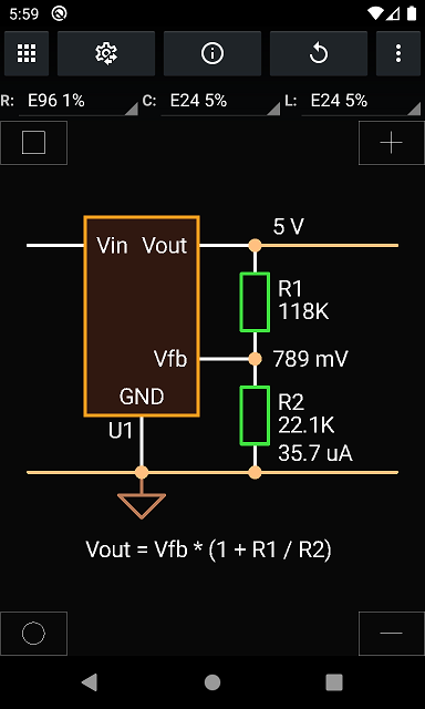
Now enter the bottom resistor value from the circuit, 10 kOhm.
现在,输入电路中的底部电阻值10 kOhm。

We see that the top resistor value must be 53.6 kOhm and not 80.6 kOhm.
我们看到最高电阻值必须为53.6 kOhm,而不是80.6 kOhm。
But what output voltage we will have at this circuit?
但是,在该电路上我们将获得什么输出电压?
Go to “Reverse of Cascade” and enter the resistor values from the circuit.
转到“级联反向”并输入电路中的电阻值。
I would not want to send 7 V to my 5 V circuit!
我不想将7 V电压发送到5 V电路!
Circuits in the datasheet use 59 kOhm and 316 kOhm for 5 V outputs, so it is an obvious mistake in this circuit.
数据手册中的电路在5 V输出时使用59 kOhm和316 kOhm,因此这是一个明显的错误电路。
But we did not verify the output voltage in the first circuit with LT8582. Let’s do this now. The reference voltage is 1.204 V and the top resistor is 45.5 K.
但是我们没有使用LT8582来验证第一个电路的输出电压。 让我们现在开始。 参考电压为1.204 V,顶部电阻为45.5K。
We see that the bottom resistor is 14.3 kOhm that matches with the previously calculated Rbottom value and the output voltage is 5.02 V, so the feedback network is correct.
我们看到底部电阻为14.3 kOhm,与先前计算的Rbottom值匹配,并且输出电压为5.02 V,因此反馈网络是正确的。
The final question is: can we trust this tool completely? I do not know.
最后一个问题是:我们可以完全信任此工具吗? 我不知道。
Electronics is complex, and equations and simplified models can be used with limitations and precautions. And still it helps and saves a lot of time.
电子设备很复杂,方程式和简化模型可以有限制和预防措施地使用。 仍然可以帮助您节省大量时间。
翻译自: https://habr.com/en/post/516676/
pmos 电源开关电路
pmos 电源开关电路_如何验证开关电源电路相关推荐
- 预充电电路工作原理_变频冰箱开关电源电路工作原理及检修思路
电冰箱的开关电源电路主要用来为电冰箱其他电路和各部件提供工作电压,市电220V 电压经过开关电源电路处理后,通过接线端子为电冰箱的用电部件供电. 下图所示为三星BCD-226型电冰箱的开关电源电路框图 ...
- 预充电电路工作原理_变频冰箱开关电源电路工作原理及检修。
电冰箱的开关电源电路主要用来为电冰箱其他电路和各部件提供工作电压,市电220V 电压经过开关电源电路处理后,通过接线端子为电冰箱的用电部件供电. 下图所示为三星BCD-226型电冰箱的开关电源电路框图 ...
- 三极管开关电路_[经验] 三极管开关电路设计指南
三极管除了可以当做交流信号放大器之外,也可以做为开关之用.严格说起来,三极管与一般的机械接点式开关在动作上并不完全相同,但是它却具有一些机械式开关所没有的特点. 图1所示,即为三极管电子开关的 ...
- b丅151组成的充电器电路_一文读懂uc3842组成的开关电源电路
UC3842组成的开关电源电路 UC3842构成的开关电源电路,220V市电由C1.L1滤除电磁干扰,负温度系数的热敏电阻Rt1限流,再经VC整流.C2滤波,电阻R1.电位器RP1降压后加到UC384 ...
- 三极管开关电路_【硬见小百科】一种三极管开关电路设计(多图)
引言三极管除了可以当做交流信号放大器之外,也可以做为开关之用.严格说起来,三极管与一般的机械接点式开关在动作上并不完全相 同,但是它却具有一些机械式开关所没有的特点.图1所示,即为三极管电子开关的基本 ...
- 真实案例分享:MOS管电源开关电路,遇到上电冲击电流超标
做硬件,堆经验. 分享一个案例:MOS管电源开关电路,遇到上电冲击电流超标,怎么解决的呢? 下面是正文部分. -- 正文 -- 最近有一颗用了挺久的MOSFET发了停产通知,供应链部门找到我们研发部门 ...
- 变频器开关电源电路实例
变频器开关电源电路实例 先看以下电路实例: 图1 东元7200PA 37kW变频器开关电源电路 图2 海利普HLPP001543B型15kW变频器开关电源电路 图1.图2电路结构和原理基本上是 ...
- 开关电源环路学习笔记(7)-BUCK电源环路仿真实验验证
前面花了三节内容,把Buck各个级的传递函数给推导出来了,只需要把它们相乘,就可以得到环路的开环传递函数了. 那有没有办法验证它们是否正确呢?这一节就来干这个事情. 验证方法 我打算使用LTspice ...
- 硬件基础:带缓启动MOS管电源开关电路
电源开关电路,经常用在各"功能模块"电路的电源通断控制,是常用电路之一. 本文要讲解的电源开关电路,是用MOS管实现的,且带缓开启功能,非常经典. 一.电路说明 电源开关电路,尤其 ...
最新文章
- ECCV 2020 论文大盘点-6D 位姿估计篇
- java 读utf-8 xml_〖JAVA经验〗JDom输出UTF-8的XML完美解决方法
- VTK:Filtering之ConnectivityFilterDemo
- windbg linux内核调试,windbg调试虚拟机XP系统
- 计算机论文答辩注意哪些问题,计算机专业论文答辩(准备和注意事项)
- excel保存超过15位数据不变科学计数法的方法
- 基于微服务架构、运行于容器中的.NET Core示例应用eShopOnContainers
- 第三天,编码设置,主键设置与删除,无关子查询,相关子查询,表与表之间的关系...
- spyder替换_Spyder 快捷键大全
- SCPPO(一):禅道的安装
- IBM 开源处理加密数据的工具集
- 广东省大学计算机应用基础考试试题,2021年广东省对口考试要做哪些题目?计算机应用基础(Windows7+office2010)周测月考单元卷...
- 垃圾邮件服务器 查询,邮件服务器ip黑名单查询
- C语言编译过程流程图
- Linux命令之火车来了
- Qt 学习(三) —— Qt 模块
- 液体特效文字AE标题模板免费下载
- Qt的跨平台的部分原理和机制
- 一个追风筝的人,追寻着什么
- SML中的local